
Flash ADC
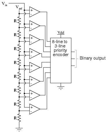
The flash ADC, or parallel A/D converter, is characterized by its rapid conversion speed, making it suitable for applications where high-speed data acquisition is critical. The architecture typically includes a bank of comparators that simultaneously evaluate the input signal against multiple reference voltages derived from a resistor ladder network. Each comparator's output is binary, indicating whether the input signal exceeds its respective reference voltage.
In a typical 3-bit flash ADC, there are eight comparators, each designed to handle a specific voltage range, producing outputs that are then fed into a priority encoder. The encoder processes these outputs to generate a binary representation of the highest active comparator. This design allows for a very fast conversion rate since all comparisons occur in parallel rather than sequentially as in other types of ADCs.
The precision voltage regulator that supplies Vref is crucial for maintaining stable reference voltages, which directly impacts the accuracy of the ADC. The design can be further optimized by selecting appropriate resistor values in the voltage divider. By using unequal resistor values, the designer can tailor the ADC's response to specific application needs, allowing for non-linear characteristics that may be advantageous in certain scenarios, such as audio processing or sensor applications where specific ranges of input voltages are more critical than others.
Despite its advantages, the flash ADC's component count increases exponentially with the number of output bits, which can pose challenges in terms of cost, size, and power consumption. For instance, an 8-bit flash ADC would require 256 comparators, making it impractical for many applications. Thus, while the flash ADC is unmatched in speed, careful consideration must be given to its complexity and resource requirements when designing systems that utilize this technology.Also called the parallel A/D converter, this circuit is the simplest to understand. It is formed of a series of comparators, each one comparing the input signal to a unique reference voltage. The comparator outputs connect to the inputs of a priority encoder circuit, which then produces a binary output.
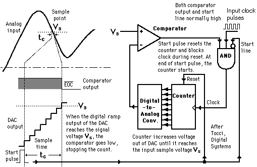
The following illustration shows a 3-bit fla sh ADC circuit: Vref is a stable reference voltage provided by a precision voltage regulator as part of the converter circuit, not shown in the schematic. As the analog input voltage exceeds the reference voltage at each comparator, the comparator outputs will sequentially saturate to a high state.
The priority encoder generates a binary number based on the highest-order active input, ignoring all other active inputs. For this particular application, a regular priority encoder with all its inherent complexity isn`t necessary.
Due to the nature of the sequential comparator output states (each comparator saturating "high" in sequence from lowest to highest), the same "highest-order-input selection" effect may be realized through a set of Exclusive-OR gates, allowing the use of a simpler, non-priority encoder: Not only is the flash converter the simplest in terms of operational theory, but it is the most efficient of the ADC technologies in terms of speed, being limited only in comparator and gate propagation delays. Unfortunately, it is the most component-intensive for any given number of output bits. This three-bit flash ADC requires eight comparators. A four-bit version would require 16 comparators. With each additional output bit, the number of required comparators doubles. Considering that eight bits is generally considered the minimum necessary for any practical ADC (256 comparators needed!), the flash methodology quickly shows its weakness.
An additional advantage of the flash converter, often overlooked, is the ability for it to produce a non-linear output. With equal-value resistors in the reference voltage divider network, each successive binary count represents the same amount of analog signal increase, providing a proportional response.
For special applications, however, the resistor values in the divider network may be made non-equal. This gives the ADC a custom, nonlinear response to the analog input signal. No other ADC design is able to grant this signal-conditioning behavior with just a few component value changes. 🔗 External reference
Related Circuits
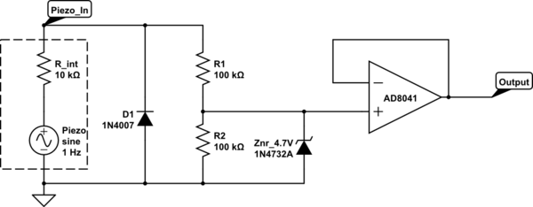
The intention is to utilize the sensor as a force sensor. It has been observed that the voltage output increases with the amount of pressure applied, although this output is only sustained for a brief period. This behavior is...
This circuit enables the brake light to flash. The default behavior occurs when power is supplied to the circuit or when the brake is engaged. The timer IC (IC2) drives current to the transistor (Q2), producing an oscillating output...
Its state is constantly changing, and this change affects the flow of current and voltage, which is visible with the two LEDs. The speed of the LED flasher can be adjusted with potentiometer P1. As an astable multivibrator, the...
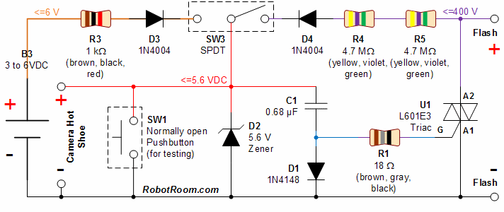
This circuit incorporates a datasheet-compliant trigger signal, reversed polarity protection, an optional test button, and the capability for battery operation. It utilizes either the U1 L601E3 or MAC97A8 triac, rated for 400 V and 1 A. When U1 is...
Analog to Digital Converter (ADC) interfacing with microcontrollers such as AVR, 8051, and PIC, including Digital-Ramp ADC, Successive Approximation ADC, Flash ADC, and basic working of an analog to digital converter. Analog to Digital Converters (ADCs) are essential components in...
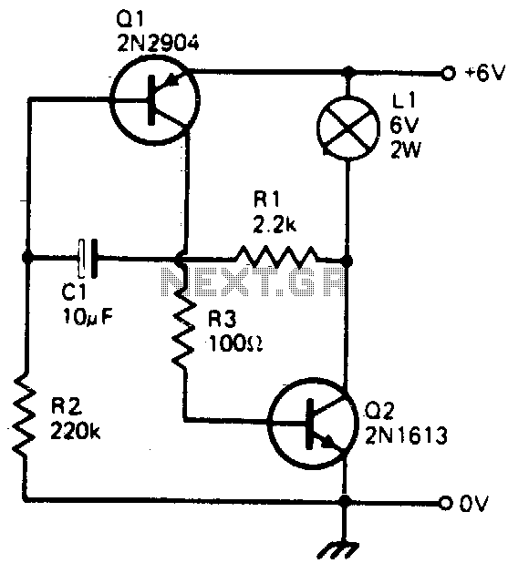
This simple circuit will flash a 6-volt lamp at a rate determined by the size of capacitor C1. It is most economical on power as it only draws current when the lamp is on. When the lamp is off,...