
ADC interface conditions high-level signals
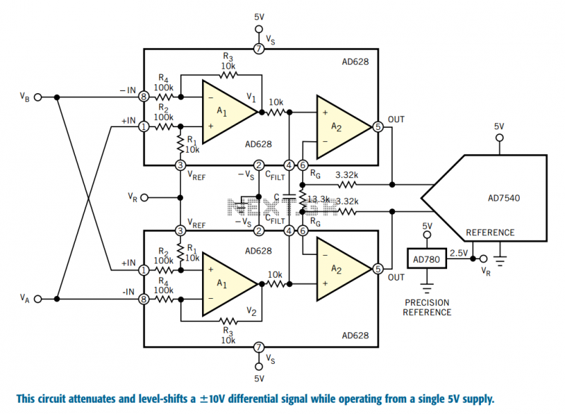
The circuit described is designed to address the challenges faced by industrial equipment designers when interfacing analog signals with ADCs. The primary objective is to manage bipolar voltages of ±10V while filtering out common-mode noise. This is achieved through the utilization of difference amplifiers that specifically reject common-mode voltages present at the inputs, VA and VB.
The reference voltage, VR, generated by the AD780, plays a crucial role in establishing the output common-mode voltage, which is essential for maintaining signal integrity. A capacitor, denoted as C, is strategically placed across the CFILT pins to implement a low-pass filter on the difference signal, V1–V2. The filter's cut-off frequency is determined by the formula fP=1/(40,000×π×C), which allows for the attenuation of high-frequency noise while preserving the desired signal frequencies.
In this configuration, the difference signal is amplified by an operational amplifier labeled A2, which provides a gain of 1.5. The overall gain of the system is calculated to be 3/10, ensuring that the output signal is appropriately scaled for the subsequent ADC input.
The circuit's architecture enhances key performance metrics, including common-mode rejection ratio (CMRR), offset voltage, drift, and noise reduction. Since the errors from each AD628 are uncorrelated, the resultant output exhibits a significantly improved signal-to-noise ratio (SNR) of 85 dB, as illustrated in the provided figures.
The integration of two AD628 difference amplifiers with an AD7450 12-bit differential-input ADC ensures effective rejection of any residual common-mode signals that may persist after amplification. The performance is further validated through waveform analysis, showcasing the common-mode error at the output of the AD628. The top waveform represents the common-mode input signal, while the middle and bottom waveforms quantify the common-mode errors measured from the outputs of the two AD628s, demonstrating the circuit's efficacy in minimizing such errors.Designers who build equipment for the industrial market share a widespread problem. At one extreme, they must build equipment that supports ±10V bipolar voltages, often riding on a high common-mode level, a requirement enforced by 30 years of legacy industrial equipment. At the other extreme, the analog signal needs conditioning to match the full-scale range of a low-voltage, single-supply ADC.
The difference amplifiers reject the common-mode voltage on inputs VA and VB. The reference voltage, VR, which the AD780 develops and the ADC and the amplifier share, sets the output common-mode voltage. A single capacitor, C, placed arcros the CFILT pins, lowpass-filters the difference signal, V1–V2.
The –3-dB pole frequency is: fP=1/(40,000×π×C). A2 amplifies the difference signal by 1.5. Thus, the total gain of this circuit is 3/10. Figure 2 shows a 10V input signal (top), the signals at the output of each AD628 (middle), and the differential output (bottom). The benefits of this configuration go beyond simply interfacing with the ADC. The circuit improves specifications such as common-mode-rejection ratio, offset voltage, drift, and noise by a factor of because the errors of each AD628 are not correlated.
The output demonstrates 85-dB SNR (Figure 3). The two AD628s interface with an AD7450 12-bit, differential-input ADC. The AD7450 easily rejects residual common-mode signals at the output of the difference amplifiers. Figure 4 shows the common-mode error at the output of the AD628. The topmost waveform is a 10V, common-mode input signal. The middle waveform, measuring 150 µV, is the common-mode error measured, differentially, from the output of the two AD628s. The bottom waveform, measuring 80 µV, is the resultant common-mode error.
Related Circuits
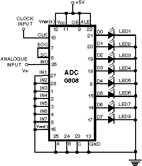
Normally analogue-to-digital converter (ADC) needs interfacing through a microprocessor to convert analogue data into digital format. This requires hardware and necessary software, resulting in increased complexity and hence the total cost. The circuit of A-to-D converter shown here is...
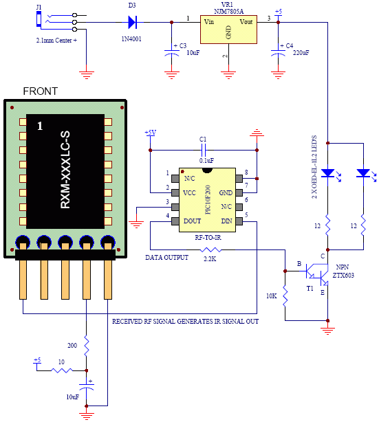
Instructions for utilizing an existing infrared transmitter from any room within the house. The concept is straightforward and operates more effectively than anticipated. This project proves to be quite useful, allowing control over devices from virtually anywhere. For instance,...
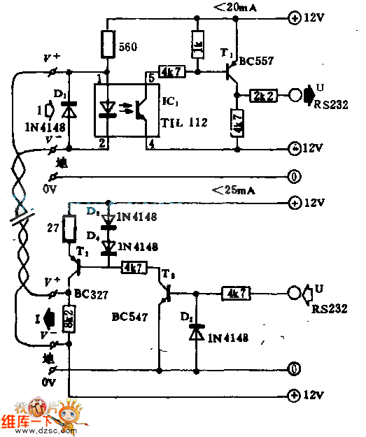
This circuitry facilitates the connection between the computer's Z RS-23 serial interface and the current ring circuitry. It converts the voltage signal of the transmission into a current signal of 20 mA, achieving a maximum speed of 1200 bits....
In this circuit, a 74HC14 hex Schmitt trigger inverter functions as a square wave oscillator to drive a small signal transistor configured as a class C amplifier. The oscillator frequency can be set to a fixed value using a...
This design note presents a simple yet feature-rich 16-watt output, universal AC input adapter power supply for modems, hubs, or similar applications. The circuit utilizes a discontinuous mode (DCM) flyback converter topology designed around ON Semiconductor's NCP1027 monolithic current...

If you are developing applications for the PIC MCU and miss debugging tools or don't have enough I/O pins for a parallel LCD interface in your design, this serial interface can help print debug messages and/or reduce the pin...