
ADC to 8051
The ADC0804, designed for 8-bit resolution, functions through a successive approximation method, allowing it to convert analog signals into digital data effectively. The device's differential analog voltage inputs enhance its versatility in various applications. The integrated clock generator simplifies the setup by eliminating the need for external clock sources, while the adjustable reference voltage enables fine-tuning of the input range, accommodating different sensor outputs.
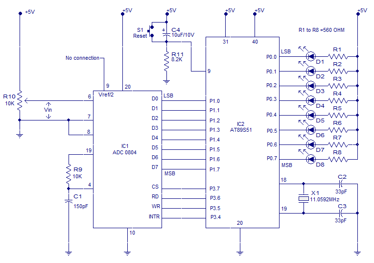
In the interfacing schematic, the microcontroller AT89S51 communicates with the ADC0804 through specific pins designated for data input and control signals. The LEDs connected to port P0 provide a visual representation of the digital output, where each LED corresponds to a bit in the 8-bit output. The use of current-limiting resistors ensures that the LEDs operate within safe current levels, preventing damage.
The control signals are vital for managing the ADC's operation. The INTR signal indicates when the conversion is complete, while the WR and RD signals control the writing and reading of data, respectively. The implementation of a reset mechanism using a push button and a debouncing circuit ensures reliable operation by preventing false triggering.
The assembly code snippet provided illustrates the initialization and operation sequence for the ADC0804. It configures the microcontroller's ports, initiates the ADC conversion, and reads the resulting digital data to display it on the LED array. The use of the CPL instruction complements the data to provide a straightforward display output, enhancing user readability.
Overall, the ADC0804's integration with the 8051 microcontroller exemplifies a typical embedded system application, demonstrating the conversion of analog signals to digital data and the subsequent display of this data in a user-friendly format.ADC (Analogto digital converter) forms a very essential part in many embedded projects and this article is about interfacing an ADC to 8051 embedded controller. ADC 0804 is the ADC used here and before going through the interfacing procedure, we must neatly understand how the ADC 0804 works.
ADC0804 is an 8 bit successive approximation analogue to digital converter from National semiconductors. The features of ADC0804 are differential analogue voltage inputs, 0-5V input voltage range, no zero adjustment, built in clock generator, reference voltage can be externally adjusted to convert smaller analogue voltage span to 8 bit resolution etc. The pin out diagram of ADC0804 is shown in the figure below. The voltage at Vref/2 (pin9) of ADC0804 can be externally adjusted to convert smaller input voltage spans to full 8 bit resolution.
Vref/2 (pin9) left open means input voltage span is 0-5V and step size is 5/255=19. 6V. Have a look at the table below for different Vref/2 voltages and corresponding analogue input voltage spans. The figure above shows the schematic for interfacing ADC0804 to 8051. The circuit initiates the ADC to convert a given analogue input, then accepts the corresponding digital data and displays it on the LED array connected at P0.
For example, if the analogue input voltage Vin is 5V then all LEDs will glow indicating 11111111 in binary which is the equivalent of 255 in decimal. AT89s51 is the microcontroller used here. Data out pins (D0 to D7) of the ADC0804 are connected to the port pins P1. 0 to P1. 7 respectively. LEDs D1 to D8 are connected to the port pins P0. 0 to P0. 7 respectively. Resistors R1 to R8 are current limiting resistors. In simple words P1 of the microcontroller is the input port and P0 is the output port. Control signals for the ADC (INTR, WR, RD and CS) are available at port pins P3. 4 to P3. 7 respectively. Resistor R9 and capacitor C1 are associated with the internal clock circuitry of the ADC. Preset resistor R10 forms a voltage divider which can be used to apply a particular input analogue voltage to the ADC.
Push button S1, resistor R11 and capacitor C4 forms a debouncing reset mechanism. Crystal X1 and capacitors C2, C3 are associated with the clock circuitry of the microcontroller. ORG 00H MOV P1, #11111111B // initiates P1 as the input port MAIN: CLR P3. 7 // makes CS=0 SETB P3. 6 // makes RD high CLR P3. 5 // makes WR low SETB P3. 5 // low to high pulse to WR for starting conversion WAIT: JB P3. 4, WAIT // polls until INTR=0 CLR P3. 7 // ensures CS=0 CLR P3. 6 // high to low pulse to RD for reading the data from ADC MOV A, P1 // moves the digital data to accumulator CPL A // complements the digital data (*see the notes) MOV P0, A // outputs the data to P0 for the LEDs SJMP MAIN // jumps back to the MAIN program END ADC 0804 has active low outputs and the instruction CPL A complements it t0 have a straight forward display. For example, if input is 5V then the output will be 11111111 and if CPL A was not used it would have been 00000000 which is rather awkward to see.
🔗 External reference
Related Circuits
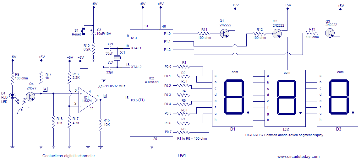
A three-digit contactless digital tachometer utilizing an 8051 microcontroller is presented for measuring the revolutions per second of rotating objects such as wheels, discs, or shafts. The tachometer can measure up to a maximum of 255 revolutions per second...
When using the internal 1.1V reference for the ADC, if the analog input exceeds 1.1V, such as 2.5V, it will not harm the microcontroller. Instead, the ADC value will clip at 0x3FF. Based on practical experience, it has been...
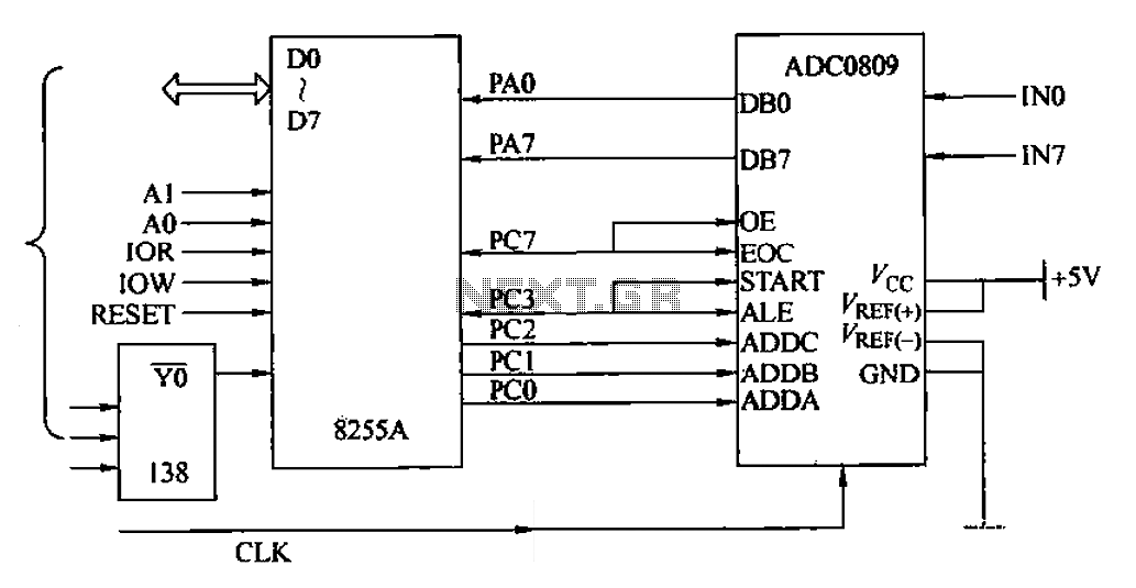
The ADC0809 is an 8-channel analog switch integrated with an 8-bit successive approximation analog-to-digital (A/D) converter. It supports the selection of eight input channels through address latch and encoder channel selection signals ADDA, ADDB, and ADDC. The address latch...
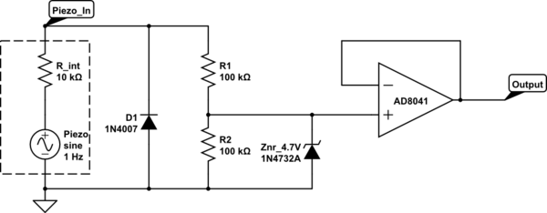
The intention is to utilize the sensor as a force sensor. It has been observed that the voltage output increases with the amount of pressure applied, although this output is only sustained for a brief period. This behavior is...
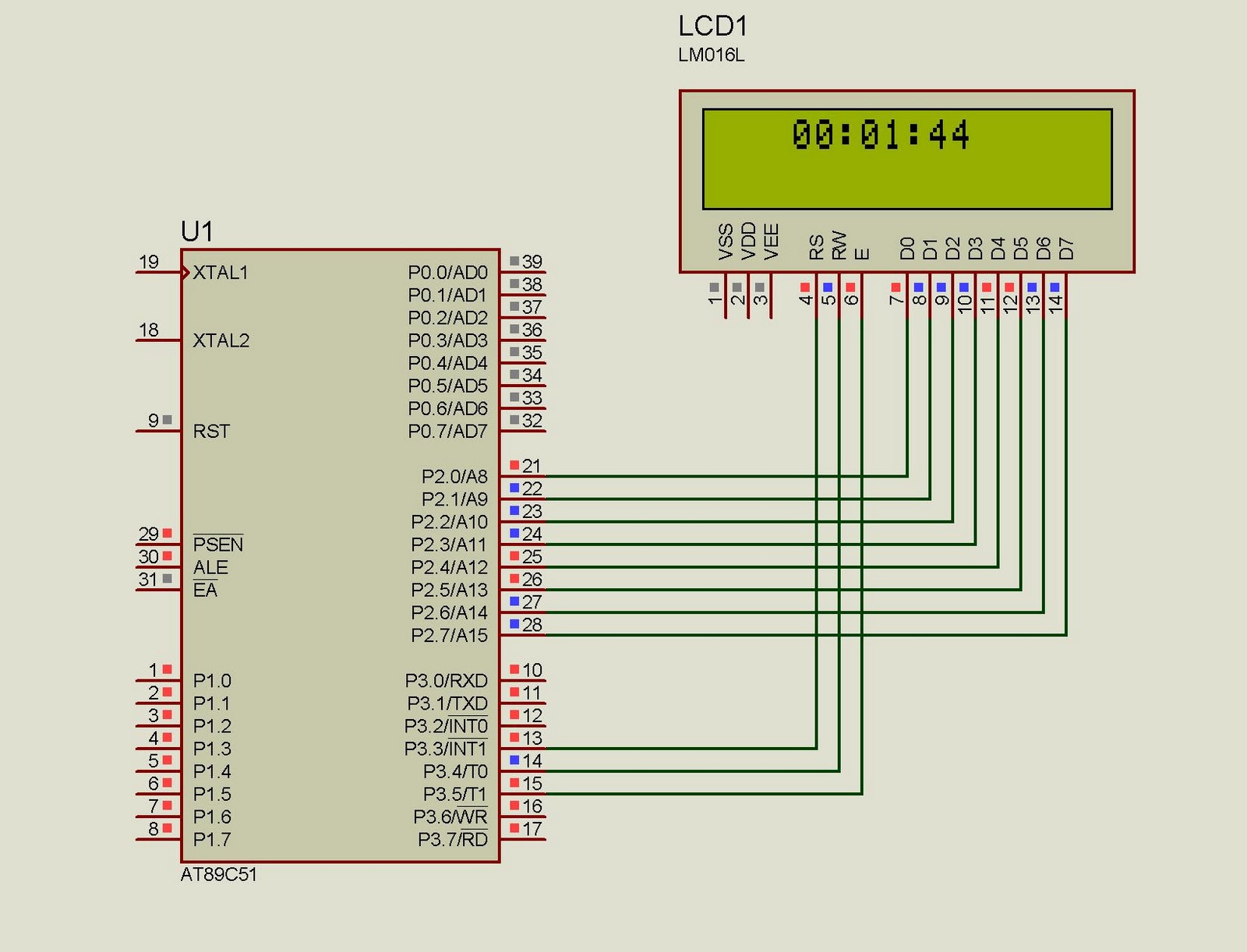
This project implements a real-time clock using the 89C51 microcontroller. The clock's data format is hours:minutes:seconds, which is displayed on a 16x2 LCD. The code has been tested and compiled using the Keil uVision compiler. The circuit diagram for...
DTMF-based Robo Car design using the 8051 microcontroller project. This project demonstrates a method to control a domestic system using the DTMF tone generated by a telephone instrument when the user presses the keypad buttons of a mobile phone...