
ADC0809 and PC bus interface circuit
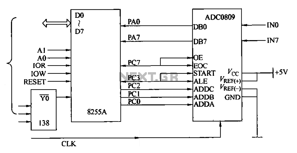
The ADC0809 is designed to provide efficient analog-to-digital conversion for a variety of applications, including sensor data acquisition and real-time signal processing. The device utilizes a successive approximation method for conversion, which allows for high-speed processing of analog signals. The integration of an address latch enables the selection of multiple input channels, making the ADC0809 suitable for systems requiring multiple analog inputs.
The operation begins when an input channel is selected via the address signals ADDA, ADDB, and ADDC. The ALE signal is then activated to latch the selected channel. Upon receiving the start conversion signal (SD), the ADC0809 initiates the conversion process. The conversion time is fixed at approximately 100 microseconds, after which the EOC signal indicates that the digital representation of the analog input is ready for retrieval.
The output data is available on the DO-D7 lines, which are driven by the tri-state latch output buffer. The tri-state feature allows the ADC0809 to share the data bus with other devices, thus enhancing the flexibility of the overall system architecture. The OE signal controls the output state; when enabled, the conversion results are presented on the data lines, while disabling the output places the lines in a high impedance state, preventing bus contention.
In practical applications, the ADC0809 can be interfaced with various microcontrollers or microprocessors, utilizing the 8255A interface chip for parallel communication. This configuration allows for straightforward integration into larger systems, enabling seamless data flow from multiple analog sources to digital processing units. The ADC0809 is thus a versatile component for engineers designing systems that require efficient and reliable analog-to-digital conversion.ADC0809 is an 8-channel analog switch with an 8-bit successive approximation A/D converter. ADC0809 8-channel analog switches can be realized now 8 to 1, an address latch and d ecoder channel selection signals ADDA, ADDB, ADDC. For selecting eight input channels a one, the address latch enable signal ALE can ADDA, ADDB, ADDC selected input channel and A/D converter connected. Eight successive approximation state D conversion analog signal converter can be input into an 8-bit binary apply, transfer to deposit conversion result output buffer tristate latch punch unit.
Positive pulse signal SD RT allows A/D converter to start the conversion, the conversion is completed after about lOOtjtS, turn after the change. EOC signal from low level to high level. Notify CPU read the data. Tri-state latch output buffer used to store the conversion result, when the output enable signal OE is high when Xu.
8-bit conversion result is output from the DO-D7, when OE is low, the data output lines DO-D7 high impedance state. Due to ADC0809 has tristate latch output buffer, which can be directly connected to the system bus. In order to facilitate or simplify the interface circuit design, usually more common parallel interface through microarrays implementation and system interfaces.
The circuit shown in FIG. ADC0809 is connected via programmable parallel interface chip 8255A achieve a circuit connected to the PC. edText, GET, ); Top class diggnum id diggnum
Related Circuits
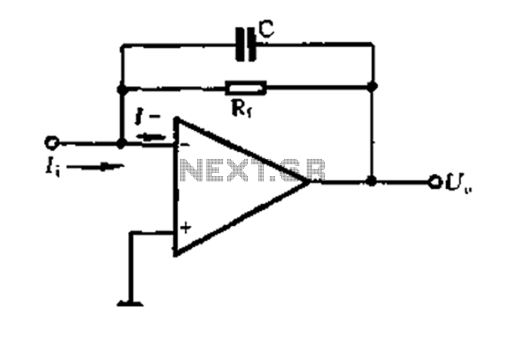
A current-voltage conversion circuit. A current-voltage conversion circuit is designed to transform an input current signal into a corresponding voltage signal. This type of circuit is fundamental in various applications, including sensor interfacing, signal conditioning, and analog-to-digital conversion processes. Typically,...

This is an application circuit for calibration known as a high voltage AC calibrator circuit. A key aspect of sine wave oscillator design is the stable control of amplitude. In this circuit, the amplitude is stabilized through servo control,...
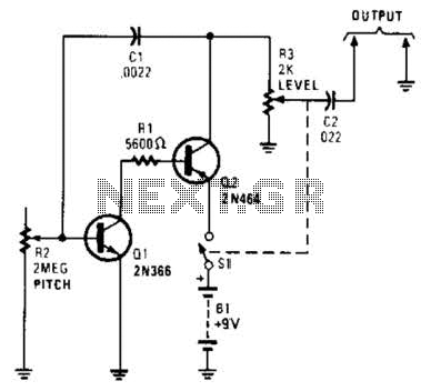
Useful for troubleshooting audio, video, and lower frequency RF amplifiers. This circuit generates a signal that is rich in harmonics. The circuit designed for troubleshooting audio, video, and lower frequency RF amplifiers is crucial for diagnosing issues in these systems....
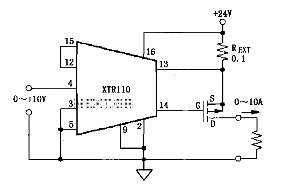
When the output current exceeds 40mA, the XTR110 requires the use of an external resistor (REXT) instead of the internal 50-ohm resistor (R9). REXT should be connected between pin 13 and pin 1. The value of REXT is determined...
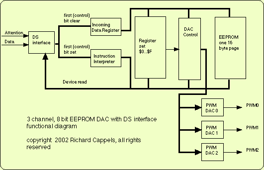
This device provides three channels of 8 bit pulse-width modulation. Output pulse duty cycle ranges from 0 to 255/256 in 255 steps. DACs may be loaded by the DS interface. DAC values may also be copied into the on-chip...
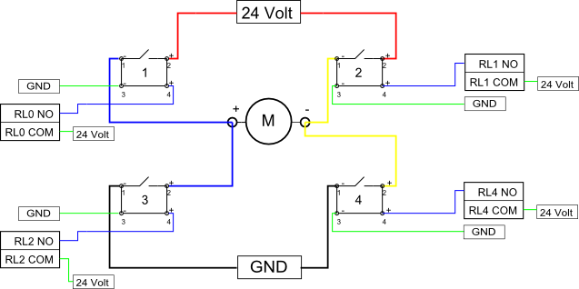
Eight solid-state relays (SSR) and an ADAM-4068 (Serial-I/O device) are utilized to wire a circuit for controlling a motor in a robotic application. The ADAM-6048 is a versatile device that facilitates control of digital inputs and outputs via RS-485...
Warning: include(partials/cookie-banner.php): Failed to open stream: Permission denied in /var/www/html/nextgr/view-circuit.php on line 713
Warning: include(): Failed opening 'partials/cookie-banner.php' for inclusion (include_path='.:/usr/share/php') in /var/www/html/nextgr/view-circuit.php on line 713