
Adjustable TTL clock
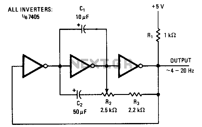
The described circuit utilizes a square-wave oscillator configuration, where the symmetry of the output waveform is crucial for maintaining a consistent duty cycle. The connection of R2 to the output of the third amplifier stage through R3 facilitates the modulation of the charging current to the capacitors, effectively allowing for precise control over the frequency of oscillation. The frequency-adjusting potentiometer R2 plays a pivotal role in this modulation, enabling the user to vary the frequency within a specified range.
The lower frequency limit of the oscillator is set by capacitor C2, which acts as a timing element in conjunction with the resistors. As the capacitance of C2 influences the time constant of the circuit, it effectively determines the minimum frequency at which the oscillator can operate. The upper frequency limit can be adjusted by changing the values of capacitor C1 and resistor R3. These components define the time constant for the charging and discharging cycles, thus impacting the maximum frequency achievable by the oscillator.
This schematic can be further optimized by selecting appropriate resistor and capacitor values based on the desired frequency range. For instance, if a higher frequency range is needed, reducing the capacitance of C1 or the resistance of R3 will result in shorter time constants, allowing the oscillator to achieve higher frequencies. Conversely, increasing C2 will lower the minimum frequency, providing flexibility in application-specific designs.
In summary, the circuit effectively provides a square-wave output with a stable 50% duty cycle across a range of frequencies from 4 to 20 hertz, with additional tuning capabilities through the careful selection of component values. This design is suitable for various applications where precise frequency control is required, such as in timing circuits, signal generators, and modulation schemes.Symmetry of the square-wave output is maintained by connecting the right side of R2 through resistor R3 to the output of the third amplifier stage. This changes the charging current to the capacitors in proportion to the setting of frequency-adjusting potentiometer R2.
Thus, a duty cycle of 50% is constant over the entire range of oscillation. The lower frequency limit is set by capacitor C2 With the components shown, the frequency of oscillation can be varied by R2 from about 4 to 20 hertz. Other frequency ranges can be obtained by changing the values of Cl and R3, which control the upper limit of oscillation, or C2, which limits the low-frequency end.
🔗 External reference
Related Circuits
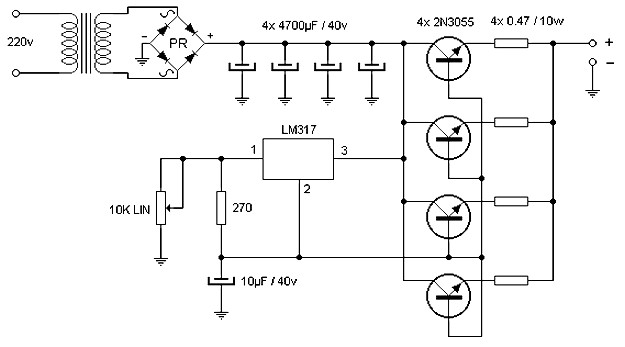
The wiring diagram illustrates that the source delivers a comparable amount of current through the parallel operation of four power transistors, which must be mounted on an effective heatsink. Voltage adjustment is achieved using an integrated LM317, which also...
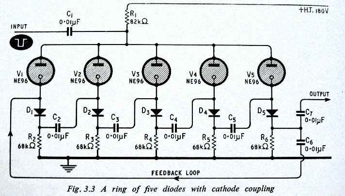
The above shows a home-built digital clock that utilizes Nixie tubes for display. Unlike most contemporary Nixie clocks, this design does not employ transistors or integrated circuits for driving the tubes. Instead, the driving logic is constructed using neon...

Usually we see Digital clock on LCD or 7 segment. But, this AVR Digital Clock which is designed by Ficara Emilio displayed on Oscilloscope. The project uses ATtiny 2313 as the main controller. What an interesting microcontroller project. Source...
Before Light-Emitting Diodes (LEDs) and Liquid Crystal Displays (LCDs), the electronics industry utilized cold-cathode tubes for displaying numbers, symbols, and characters. Although referred to as "tubes," they differ from "radio tubes" in that they lack a heater wire to...

The clock displays time in 5-minute intervals, with adjustable hour and minute settings. There is no alarm feature or AM/PM indicator. The clock face is constructed from two pieces of linoleum glued together for added thickness, though floor tiles...
The 20-MHz clock is phase-locked to the 10-MHz NuBus clock of Apple's Mac II. It employs simple and cost-effective CMOS circuitry to generate square waves at 10 MHz and 20 MHz. The output duty cycle settings are not affected...