
Aircraft band / AM Receiver with PIC16F84

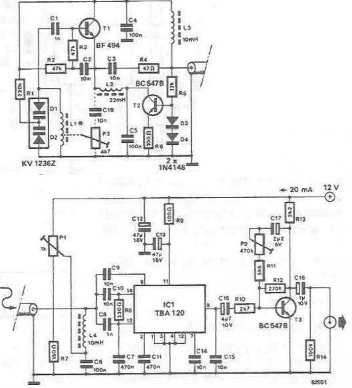
To the left, you will find the preamplifier. It is based on a dual-gate FET (You can use almost any dual-gate FET). At Gate 1, we have the antenna input. L1 and C1 will tune the antenna for best performance. To find a super perfect antenna match, you can solder the antenna to a tap-point of L1. Gate 2 is biased to give high gain. At the drain, you will find another tuned circuit L2 and C2. This circuit should also be tuned for best performance. L2 is a transformer slug-tuned inductor. An inductor with an AL value of 7 with 5 turns primary will yield 175 nH. This inductor transforms the RF to the secondary side with 3 turns which is connected to mixer 1.
In the MC13136, an oscillator is found at pins 1 and 2. This oscillator is connected to mixer 1. A tuned circuit connected to C3 and L3 enhances this oscillator. To make this oscillator voltage-controlled, a varicap diode is placed between pins 24 and 23. The capacitance of this diode is dependent on the voltage applied across it. A small 10 pF capacitor connects the varicap and C3, allowing frequency adjustment by applying a voltage to pin 24.
In mixer 2, the RF signal flows from mixer 1 through the ceramic filter into mixer 2. At pins 5 and 6, a fixed oscillator with a crystal operates at 10.245 MHz. The 455 kHz IF passes through a ceramic filter to the AM demodulator. At pin 15, a voltage indicates the strength of the input RF signal (RSSI), which can control a squelch unit.
The PLL synthesizer is a critical component in this design. At pin 2, a 10 kΩ resistor is connected to ground to amplify the oscillation current. A fraction of the oscillation energy passes through a 10 pF capacitor to a FET buffer, preventing glitches from the PLL from affecting the VCO and avoiding excessive loading on the VCO. The VCO frequency is amplified at pin 5 of the PLL, while pin 3 serves as the phase detector output. The PLL regulates the current at this pin, and with capacitors and resistors, a voltage is fed back to the varicap at pin 24 of the MC13136 through a 100 kΩ resistor. Monitoring this voltage with a voltmeter will demonstrate how the system maintains frequency lock. Aircraft communication is still AM modulated and the frequency is about 110-125 MHz. What differ this construction from my two previous is that I have implemented many blocks into one circuit and therefore I will have superior performance with less components. The receiver is working with a Frequency Synthesizer which gives a very stable reception and it is easy to change frequency as well.
The RF signal is first amplified before it enters mixer 1. To mixer1 is also a VCO (Voltage Controlled Oscillator). The tuning voltage to the oscillator is controlled by the PLL synthesizer. There is also a feedback from the output of the VCO to the PLL synthesizer. The synthesizer will control the VCO-voltage until the frequency is locked to the desired frequency you have programmed into the PIC circuit. The product of the mixer 1 is filtered into a standard 10.7MHz ceramic filter and then enter mixer 2.
At mixer 2 the RF will be mixed with a constant frequency from a crystal (10.245MHz). The product will enter a new ceramic filter and finally into a AM demodulator which brings out the audio. To the left you will find the preamplifier. It is based on a dualgate fet (You can use almost any dualgate fet). At Gate 1 we have the antenna input. L1 and C1 will tune the antenna for best performance. To find super perfect antenna match you can solder the antenna to a tap-point of L1. I can not tell you where to put the tap, you have to experiment yourself. Gate 2 is biased to give high gain. At drain you will find another tuned circuit L2 and C2. This circuit should also be tuned for best performance. I have chosen L2 to be a transformer slugtuned Inductor. I have an inductor with AL value of 7. With 5 turns primary I will get 5*5*7=175nH. This inductor transform the RF to the secondary side 3 turns which is connected to mixer 1. Mixer 1 and Mixer 2: In the MC13136 you will find an oscillator at pin 1 and 2. This oscillator is connected to mixer 1. To pin 1 and 2 is a tuned circuit connected C3 and L3. How to make this oscillator voltage controlled? Between pin 24 and 23 is a varicap diod. The capacitans of this diod is dependent of the voltage over it. Look at the schematic and you will find a small 10pF capacitor connecting the varicap and the C3. So, by applying a voltage to pin 24 you will now be able to change the frequency a few MHz. Forget about that now and look at mixer 2. You see how the RF signal goes from mixer 1 through the ceramic filter into mixer 2. At pin 5 and 6 you will find a fixed oscillator with a crystall. This oscillator is always 10.245MHz (hopefully). The 455KHz IF is now passing a ceramic filter and to the AM demodulator. At Pin 15 you will have a voltage depending on the strength of the input RF signal (RSSI). This voltage can control a squelsh unit. PLL synthesizer: Many people get scared when it comes to PLL stuff. Don't worry I will explain to you. Earlier I told you that the oscillator was at pin 1 and 2. Well, at pin 2 I have added a 10k resistor to ground because I want to amplify the oscillation current. A fraction of the oscillation energy slips away through a 10pF capacitor down to a FET buffer. This buffer is needed because I don't want glitches from the PLL go back into the VCO and I don't want to load the VCO to much either.
At pin5 of the PLL I will have the VCO frequency amplified. Pin 3 of the PLL is the Phase detector output. The PLL will regulate the current at this pin and with some capacitor and resistor I will have a voltage which is feed back to the varicap at pin 24 of the MC13136 through a 100k resistor. If you want you can probe (schematic Vtune) this voltage with a voltmeter and you will see how it keeps the frequency locked.
🔗 External reference
Related Circuits
The Field Effect Transistor (FET) exhibits a high input impedance, allowing the construction of high input impedance amplifiers. However, as a FET amplifying device, the distributed capacitance and the Miller effect significantly increase input capacitance at high frequencies. Furthermore,...
The Infrared IR Receiver circuit consists of a phototransistor, a microcontroller, and an amplifier. Understanding the data transfer between these three components is essential for successfully operating the circuit. The phototransistor receives digitally encoded data from an IR emitting...
The circuit requires an RF input, which can be sourced from either a long wire or a loop antenna. The preamplifier operates within a frequency range from 550 kHz (Medium Wave) up to 30 MHz in the shortwave band....

Frequency shift keying (FSK) is a widely used digital modulation technique for data transmission. Common applications of FSK modulation encompass both wired and wireless data transmission, as well as infrared remote controls for consumer electronic devices. FSK demodulation can...
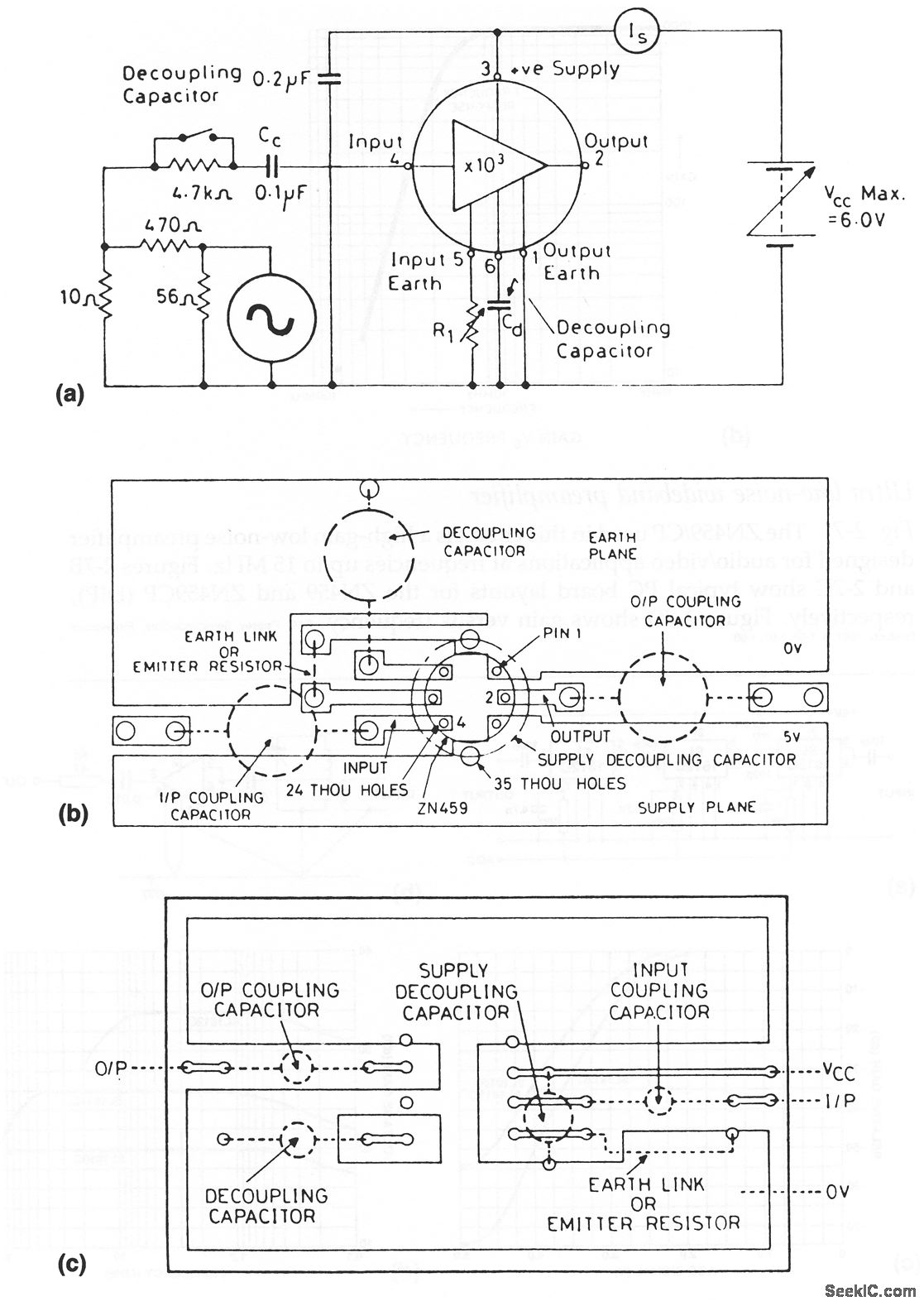
The ZN459/CP utilized in this circuit is a high-gain, low-noise preamplifier intended for audio and video applications at frequencies reaching up to 15 MHz. Figures 2-7B and 2-7C illustrate typical printed circuit board layouts for the ZN459 and ZN459CP...
The tuning stage of this long-wave and medium-wave radio receiver also functions as an active antenna, which can be optimally positioned for the best reception. The circuit is completely independent from the receiver, which includes a demodulator that provides...