
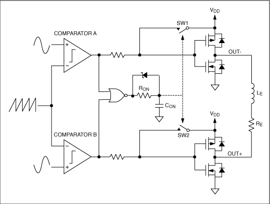
amplifier How to improve nasty form clipping behavior in differential input stage

The schematic represents an amplifier circuit designed to enhance low-level signals. The primary component, typically a bipolar junction transistor (BJT) or operational amplifier (op-amp), is configured in a way that allows for signal amplification while maintaining fidelity at lower input levels. The circuit's gain is set to achieve a tenfold increase in output voltage for a 0.1V input, resulting in an output of 10V, which is suitable for many applications requiring signal conditioning.
However, the circuit's performance under larger input signals reveals a critical limitation. The abrupt drop in output voltage from around 16V to near zero indicates that the amplifier may be entering saturation or clipping conditions. In saturation, the amplifier cannot provide a linear output, leading to distortion of the signal. This behavior is particularly pronounced during the positive half cycle of the input waveform, suggesting that the design may lack adequate headroom for larger signals, causing the output to be limited by the power supply voltage or the amplifier's inherent characteristics.
The presence of hysteresis in the recovery phase further complicates the amplifier's behavior. Hysteresis refers to the lag between the input and output signals during transitions, which can lead to undesirable effects, such as increased distortion and instability in the output signal. This could be a result of feedback mechanisms within the circuit, where the output does not immediately return to its original state after the input signal decreases, thus affecting the overall performance of the amplifier.
To address these issues, modifications to the circuit design may be necessary. This could include adjusting the biasing conditions, increasing the power supply voltage, or implementing feedback stabilization techniques to improve linearity and reduce hysteresis effects. Additionally, selecting components with appropriate ratings and characteristics will enhance the amplifier's ability to handle larger signals without compromising performance.The amplifier in the following schematic, when simulated, shows that it can cleanly amplify a signal with 0. 1V amplitude to 10V. When driven with a larger signal, though, the behavior is very nasty in the positive half cycle. The output suddenly dives from around 16V to the neighborhood of zero. Moreover, the recovery shows hysteresis. 🔗 External reference
Related Circuits
Ultra-low EMI, mono and stereo, Class D audio power amplifiers deliver Class AB performance while maintaining Class D efficiency. Maxim's spread spectrum modulation (SSM) combined with third-generation EMI reduction techniques minimizes EMI radiation by decreasing the high-frequency components of...
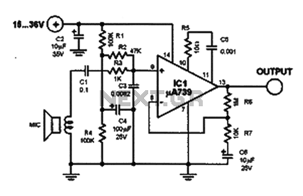
This microphone preamplifier utilizes the low-noise integrated circuit (IC) uA739. It serves as a practical example of designing an effective preamplifier for dynamic microphones. The IC contains two identical integrated preamplifier circuits, with the second preamp functioning in the...
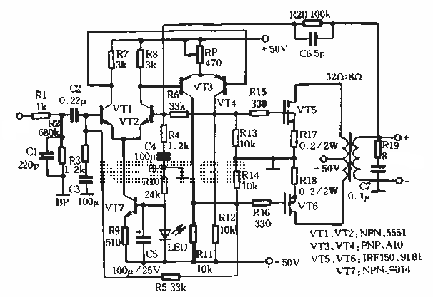
This article describes a transformer-based output FET amplifier, with tonal characteristics similar to those of tube amplifiers. It introduces various effects that are significant for audio enthusiasts. Power amplifier specifications include a rated output power of 50W (with an...
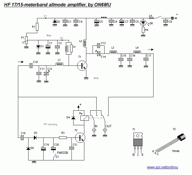
This project aims to provide a 0.55-watt input that can easily be amplified to a 10-watt output. The two linear amplifiers are designed for use with QRP SSB/CW/FM/AM transmitters on the amateur bands of 15 and 17 meters and...
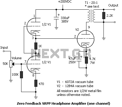
To get a low output impedance I needed to use quite a high step-down ratio (20:1); after all, the amplifier may be used with headphones of lower impedance than the 300 Ohms of the HD600. The output valve is...
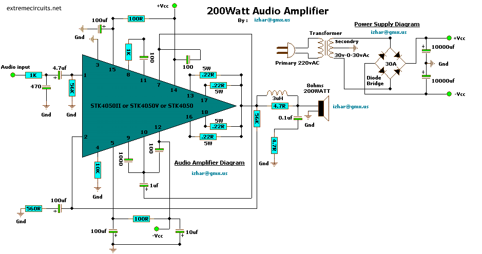
This complete aerial quality, low noise address audio amplifier is based on the Hybrid Integrated Circuit STK4050 manufactured by Sanyo. The circuit incorporates all necessary components and has a maximum output power of 200W. It features an onboard power...