
AN7415 FM Stereo Demodulator
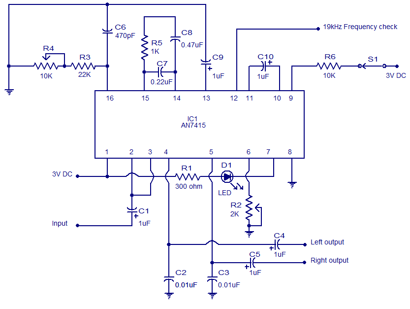
The stereo FM PLL demodulator circuit utilizing the AN7415 IC is designed to effectively demodulate FM signals and provide stereo audio output. The input coupling capacitor C1 ensures that any DC offset from the input signal does not interfere with the demodulation process. The LED D1 provides a visual indicator of the circuit's operational status, while R1 protects the LED by limiting the current flowing through it.
The output channels are decoupled by C4 and C5, which prevent any DC voltage present in the amplifier from affecting the audio output. Bypass capacitors C2 and C3 are critical for reducing noise, ensuring that the audio output remains clear and free from unwanted interference. The adjustment potentiometer R2 allows for fine-tuning of channel separation, which is essential in stereo applications to prevent crosstalk between left and right audio channels.
The low-pass filter network formed by R5, C7, and C8 is crucial for smoothing the output from the internal DC amplifier, providing a clean signal that enhances audio fidelity. The filter capacitor C10 stabilizes the internal Schmitt trigger, while C9 addresses any transient wave surges, ensuring the stability of the circuit during operation.
The time constant for the VCO circuit is determined by the combination of resistors R3, R4, and capacitor C6. The potentiometer R4 allows for precise frequency adjustments of the VCO, which is critical for maintaining synchronization with the incoming FM signal. The availability of a 19 kHz control signal at pin 12 of the AN7415 is significant for applications requiring a reference frequency, such as in stereo decoding.
Finally, switch S1 provides a user-friendly interface for toggling the forced mono mode, allowing users to choose between stereo and mono audio output based on their listening preferences or requirements. This circuit exemplifies the integration of various electronic components to achieve a sophisticated audio processing solution in FM demodulation.Welcome to the weblog where we discuss about electronic circuits schematics, PCB design, diy kits and electronic projects diagrams. The circuit shown is a stereo FM PLL demodulator designed based on the AN7415. C1 is the input coupling capacitor to block any DC voltage present on the multiplexed input signal. LED D1 is an LED and R1 is the curren t limiting resistor. C4 and C5 are DC decoupling capacitors to the output channels left and right. C2 and C3 are bypass capacitors for noise output channels left and right. POT R2 can be used to adjust the separation between channels. The resistor R5 and capacitors C7 and C8 form a network of low-pass filter for the internal DC amplifier circuit (see block diagram AN7415). C10 is a filter capacitor for the internal amplifier circuit Schmitt trigger IC. C9 is a filter capacitor for the circuit wave surge inside the AN7415. Resistor R3, R4 and capacitor C6 POT set the time constant of internal VCO circuit. Therefore POT R4 can be used to adjust the frequency of the VCO. A control signal 19KHz frequency is available in 12 pin IC. The switch S1 can be used to activate and deactivate the forced mono. 🔗 External reference
Related Circuits
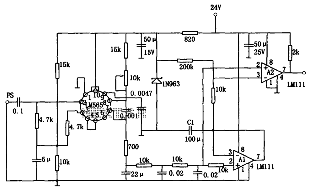
The sensitive frequency demodulation circuit utilizes the LM565 integrated circuit in a phase-locked configuration, allowing it to track frequency offsets across a wide range. However, at small frequency offsets, the signal can produce a minimal demodulated output, causing the...
The TA1284FN is a TV tuner integrated circuit (IC) that combines a mixer and oscillator for VHF and CATV bands, a mixer and oscillator for the UHF band, and an intermediate frequency (IF) amplifier into a single chip. It...

This circuit is a Phase-Locked Loop (PLL) system designed to function as an FM demodulator. The output of the Voltage-Controlled Oscillator (VCO) tracks the FM signal, and since the input voltage of the VCO is proportional to its output...
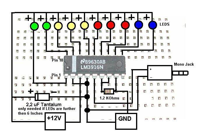
This is a concise guide for constructing a stereo VU meter utilizing the LM3915/LM3916 integrated circuits. The LM3916 is designed to convert analog voltage levels into visual representations through the activation of 10 LEDs, LCDs, or vacuum fluorescent displays,...
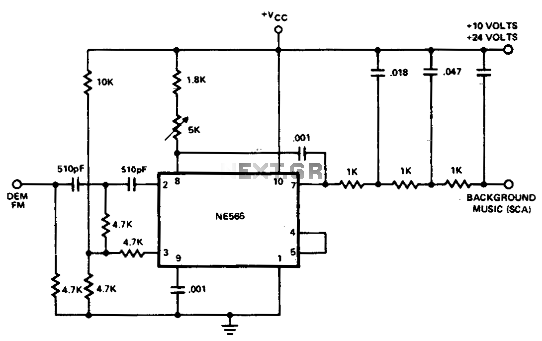
This application involves the demodulation of a frequency-modulated subcarrier from the main channel. A popular example utilizes a Phase-Locked Loop (PLL) to recover the Subsidiary Carrier Authorization (SCA) signal, which is used for storecast music, from the combined signal...
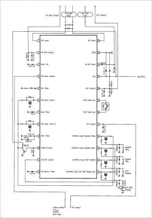
The TDA9813T is an integrated circuit designed for processing vision intermediate frequency (IF) signals and dual frequency modulation (FM) demodulation of sound. It operates with a single reference QSS-IF in television (TV) and video cassette recorder (VCR) applications, specifically...