
Sensitive frequency demodulator LM565 LM111
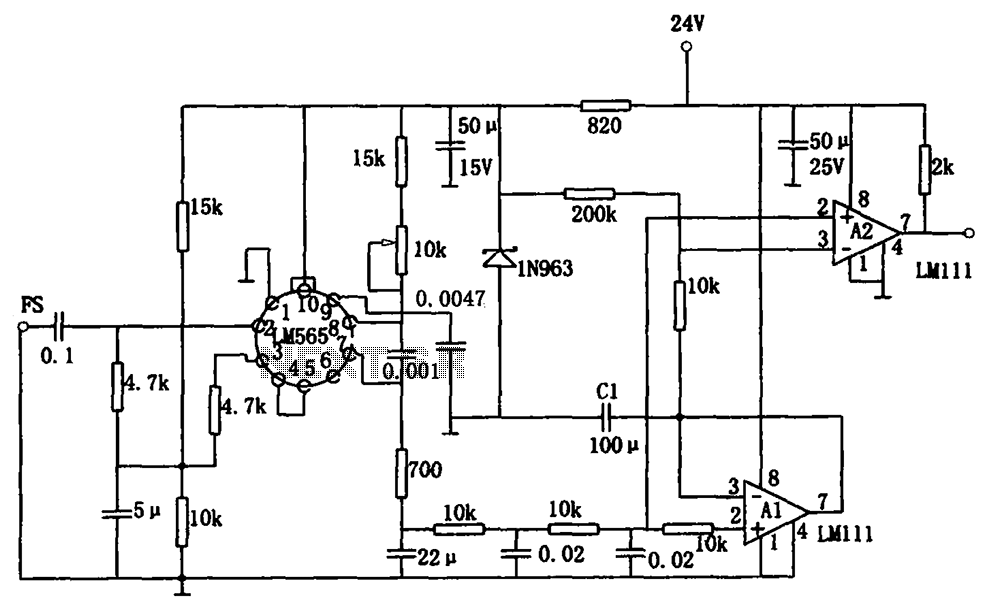
The sensitive frequency demodulation circuit is designed to provide reliable performance even in challenging conditions where frequency offsets are minimal. The use of the LM565 IC in a phase-locked loop configuration enables the circuit to lock onto the input frequency and track variations effectively. The addition of the DC regeneration section is crucial for maintaining the integrity of the demodulated signal, especially when the output signal is weak.
In this circuit, the LM111 comparator plays a vital role in comparing the demodulated output signal against a reference voltage to determine the presence of frequency deviations. The unique configuration where the input to pin A2 is derived from the peak hold circuit at A1 allows for improved stability. This design ensures that even when the output signal from the demodulator is low, the capacitor C1 can discharge effectively, maintaining a consistent voltage level that the comparator can use for accurate frequency detection.
The peak hold circuit is essential for capturing the maximum value of the demodulated signal during the modulation interval, which is then used to inform the comparator of the signal state. The low output impedance of A1 ensures that the peak hold circuit can quickly respond to changes in the input signal, thus enhancing the overall responsiveness of the demodulation circuit.
In summary, the sensitive frequency demodulation circuit with LM565 and LM111 components is engineered to deliver precise frequency tracking capabilities while mitigating the effects of signal drift and ensuring stable operation under varying input conditions. This robustness makes it suitable for applications requiring high fidelity in frequency demodulation, such as communication systems and signal processing tasks. As shown for the sensitive frequency demodulation circuit. The circuit uses IC LM565 phase-locked configuration, can track the frequency offset over a wide frequency range. How ever, at small offsets the signal, due to the small demodulated output signal, the voltage controlled oscillator will drift a drift of the operating point of the comparator generates an error. This circuit is to overcome the above drawbacks, the circuit plus a DC regeneration section, which can stably work for a small deviation signal.
FIG, the demodulation circuit and general frequency demodulation circuit LM565 and LM111 comparator constituted substantially the same. The difference is that this circuit A2 pin input signal is not removed from the LM565 feet, but was removed from the peak hold circuit A1.
During the interval of the FM input signal, the output of A1 is low, thus holding the capacitor C1 is discharged A1 low output impedance, and the peak hold signal. With this direct approach to regeneration, despite the presence of a voltage controlled oscillator drift, but the peak hold circuit output can be tracked, so that the comparator can work.
Related Circuits
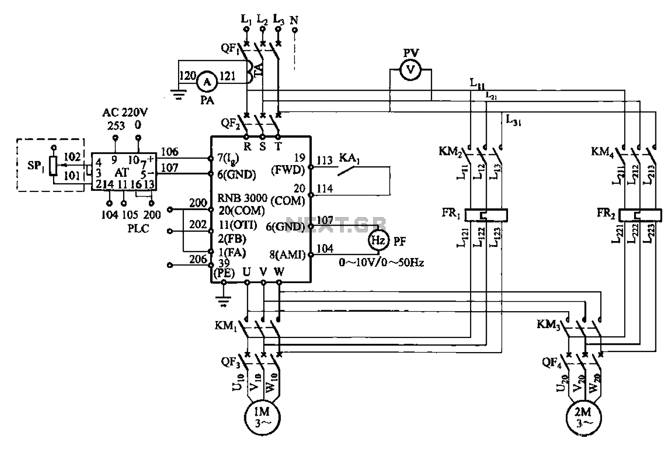
A control circuit for two motors, specifically for frequency control in a constant pressure water supply system, is illustrated in Figure 5-23. The circuit includes fault output terminals labeled 1 and 2, analog feedback current input terminals labeled 6...
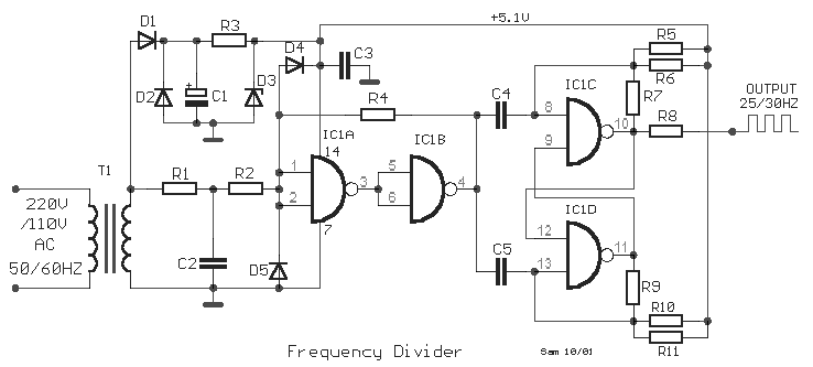
This is a classic frequency divider by two, implemented using a T-flip flop circuit, specifically with IC1 [4011]. In this circuit, the frequency from the network, after limiting the negative half-period of the sine wave and transforming it into...
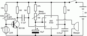
This circuit illustrates the NE555 timer used in a light-sensitive alarm sensor circuit diagram. Features include the ability to detect a sudden shadow falling on the sensor. The NE555 timer is a versatile integrated circuit widely utilized in various timing,...

A project is underway that necessitates the conversion of a 0-10V DC supply into a linear frequency range in the form of a square wave. The project involves designing a circuit that takes a direct current (DC) voltage input ranging...
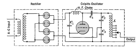
High frequencies are defined as those above 50,000 cycles per second. For industrial power supplies, the Golpitts circuit or the coupled-grid self-excited oscillator circuit is most commonly used. In either circuit, the alternating supply voltage is stepped up through...
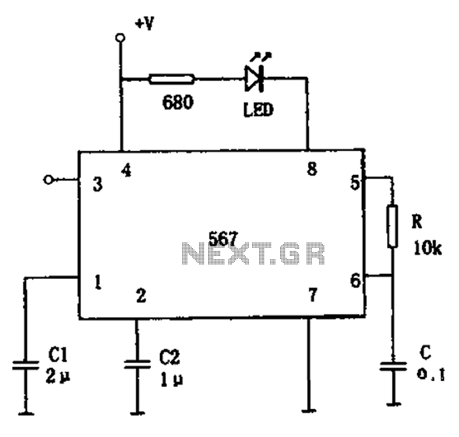
The FM demodulation circuit is illustrated in Figure 567. The FM signal is input at pin 3, and the demodulated signal is output from pin 5. The center frequency of the FM demodulation circuit is determined by the formula...