
Analog De-Glitch Circuit Circuit

This circuit functions effectively for capturing and holding low-frequency signals, making it suitable for various applications in measurement and data logging. The use of a tracking sample-and-hold configuration allows for accurate representation of transient signals, which is crucial in scenarios where signal integrity is paramount. The buffering and inversion of the input signal by IC1a ensures that the subsequent processing stages receive a stable and appropriately conditioned signal.
The differentiation stage provides the necessary signal transitions that are critical for the operation of the comparators. The adjustable reference levels set by VR1 and VR2 are essential for preventing false triggering, which could lead to erroneous outputs. The design incorporates two comparators to enhance reliability, as either can trigger the monostable multivibrator IC3, thereby providing a fail-safe mechanism.
The integration function performed by IC1b during the inactive state of IC3 allows for continuous tracking of the input signal, ensuring that the circuit can respond dynamically to signal changes. The transition to a hold state upon triggering of the monostable is a key feature, allowing for the output to maintain a stable value that can be processed further.
The output waveform's ability to be filtered enhances its utility, allowing for the removal of unwanted harmonics that may arise from the switching action of the monostable. This capability is particularly useful in applications where signal fidelity is critical, such as in audio processing or precision measurement systems.
The consideration of the monostable period is also significant; optimizing this duration relative to the input signal characteristics can lead to improved performance. A shorter monostable period relative to the signal waveform allows for more accurate representation of the signal's dynamics, which is beneficial in high-speed applications.
Overall, this circuit design exemplifies a robust approach to low-frequency signal processing, balancing the need for accurate signal tracking with the ability to hold and filter signals effectively. Low-frequency signals produced by transducers, measurement equipment, or data loggers often appear like the first waveform in the figure. The circuit shown operates as a tracking sample-hold, and the transients are replaced in the output by the stored value of the current signal at the instant of the transient.
The input signal is buffered and inverted by ICla, and the differentiated result shown at 2 applied to the inputs of two comparators IC2-a and IC2-b. VR1 and VR2 set levels to prevent false or unnecessary operation. Either comparator output triggers the mono IC3 from positive or negative signal transients. When IC3 has not been triggered, TR1 and TR2 *p` channel JFETs are on, and IClb operates as an integrator with a high leakage, and tracks the input signal. When the mono is triggered as at 3, TR1 and TR2 turn off and the previous signal value is held constant, as shown at 4.
The resulting output waveform can then be easily filtered to remove the harmonics from the restoring step at the end of the mono period, if needed. The signal range is approximately 5 V, depending on the transient amplitude and polarity. The mono period shown is 100 mS, but this can be optimized in practical applications. The shorter the mono period in relation to the signal waveform, the better the quality of the result.
Related Circuits
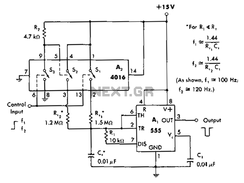
A circuit diagram controls the timing based on the input line state. When the input line is high, the 4016 CMOS analog switches select the timing of a 1.5 megohm resistor (Rt1) to produce negative output pulses at a...
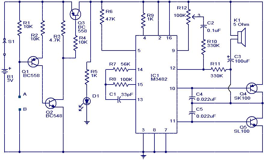
This circuit is a simple musical alarm that generates a tone when water or another conductive liquid touches the two sensor wires provided. It utilizes four transistors and a melody generator integrated circuit (IC) M3482. When water bridges the...
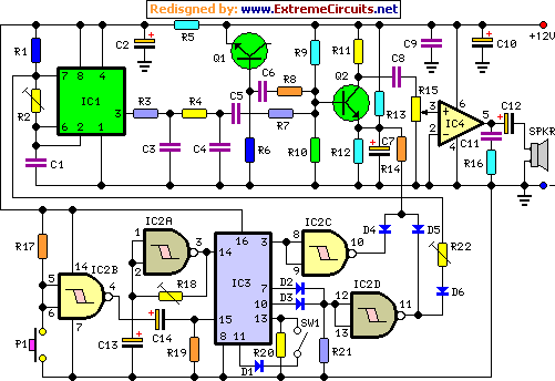
This circuit generates a two-tone effect similar to the cuckoo song. It can be utilized for doorbells or other applications due to its integrated audio amplifier and loudspeaker. When used as a sound effect generator, it can be connected...
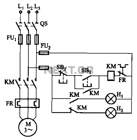
The circuit illustrated in FIG. 3 + 20 features SBi as the start button, SB2 as the stop button, Hi for run lights, and Hz for down lights. The subsequent circuit description aims to prevent tediousness by omitting the...

The TDA6106Q test circuit, as depicted in the provided figure, operates with a feedback factor of 1/116. The input signal, Vin, is received from the input network consisting of resistors R1, R9 and capacitors C1, C2. The TDA6106Q IC...
A crystal oscillator circuit comprises various gates as illustrated in the provided figures. Figure (A) represents a crystal oscillator circuit operating at 1 MHz, while figure (B) depicts a 20 MHz crystal oscillator circuit. Figure (C) shows a variable...