
astable circuit produce pulses

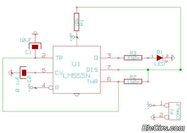
The SE555/NE555 timer IC is a versatile component widely used in various timing, pulse generation, and oscillator applications. It operates in three primary modes: monostable, astable, and bistable. In monostable mode, the timer generates a single output pulse in response to a trigger input, with the duration of the pulse determined by external resistors and capacitors. In astable mode, the timer continuously oscillates between high and low states, functioning as an oscillator. The frequency and duty cycle of the output waveform can be adjusted through external components connected to pins 6, 7, and 5. Bistable mode allows the timer to act as a flip-flop, where the output state can be toggled between high and low by applying triggers to pins 2 and 4.
The internal architecture of the 555 timer includes two voltage comparators, a flip-flop, a discharge transistor, and a resistor divider network. The voltage comparators compare the input voltages at pins 2 and 6 against reference levels set by the internal resistor divider. The output of the flip-flop controls the discharge transistor, which discharges the timing capacitor connected to pin 6 when the threshold voltage is exceeded, thus determining the output state.
In practical applications, the 555 timer can be used for generating clock pulses, timing delays, frequency modulation, and as a simple light flasher or tone generator. Its ease of use, combined with a robust design, makes it a staple in both educational and professional electronics projects. Proper consideration of the supply voltage, external component values, and pin configurations is essential for achieving the desired operational characteristics in any given application.This is circuit that first introduced by Signetics Corporation as the SE555/NE555 about 1971. Pin connections and functions: (See schematic below for basic circuits). Pin 1 (Ground) The ground (or common) pin is the most-negative supply potential of the device, which is normally connected to circuit common when operated from positive supply vo ltages. Pin 2 (Trigger) This pin is the input which causes the output to go high and begin the timing cycle. Triggering occurs when the trigger input moves from a voltage above 2/3 of the supply voltage to a voltage below 1/3 of the supply. This is the figure of the circuit. For example using a 12 volt supply, the trigger input voltage must start from above 8 volts and move down to a voltage below 4 volts to begin the timing cycle.
The action is level sensitive and the trigger voltage may move very slowly. To avoid retriggering, the trigger voltage must return to a voltage above 1/3 of the supply before the end of the timing cycle in the mono stable mode. Trigger input current is about 0. 5 micro amps. Pin 3 (Output) The output pin of the 555 moves to a high level of 1. 7 volts less than the supply voltage when the timing cycle begins. The output returns to a low level near 0 at the end of the cycle. Maximum current from the output at either low or high levels is approximately 200 mA. Pin 4 (Reset): A low logic level on this pin resets the timer and returns the output to a low state. It is normally connected to the + supply line if not used. Pin 5 (Control) This pin allows changing the triggering and threshold voltages by applying an external voltage.
When the timer is operating in the astable or oscillating mode, this input could be used to alter or frequency modulate the output. If not in use, it is recommended installing a small capacitor from pin 5 to ground to avoid possible false or erratic triggering from noise effects.
Pin 6 (Threshold) Pin 6 is used to reset the latch and cause the output to go low. Reset occurs when the voltage on this pin moves from a voltage below 1/3 of the supply to a voltage above 2/3 of the supply. The action is level sensitive and can move slowly similar to the trigger voltage. Pin 7 (Discharge) This pin is an open collector output which is in phase with the main output on pin 3 and has similar current sinking capability.
Pin 8 (V +) This is the positive supply voltage terminal of the 555 timer IC. Supply-voltage operating range is +4. 5 volts (minimum) to +16 volts (maximum). 🔗 External reference
Related Circuits
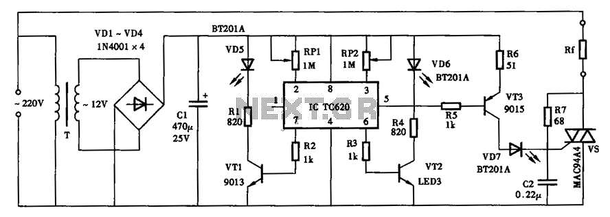
The thermostat can be set, and it specifies the lower limit of the circuit diagram. The thermostat in the circuit is a critical component used to regulate temperature by controlling the heating or cooling system. It operates by comparing the...
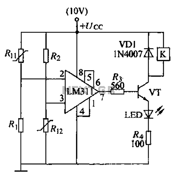
A boiler control circuit is designed to regulate the temperature of water in a hot water heating system. This circuit typically utilizes a comparator's comparison function to manage the heating equipment. The circuit includes a thermistor that forms a...
Second Stage Joule Thief Circuits The second stage Joule Thief circuit is an advanced iteration of the basic Joule Thief design, which is primarily used to extract energy from low-voltage sources, such as depleted batteries. This circuit is particularly effective...
This is a very simple 555 timer circuit that serves as a straightforward theft deterrent, which may be just as effective. The idea is to have a flashing red LED indicate that your car is protected. This device can...
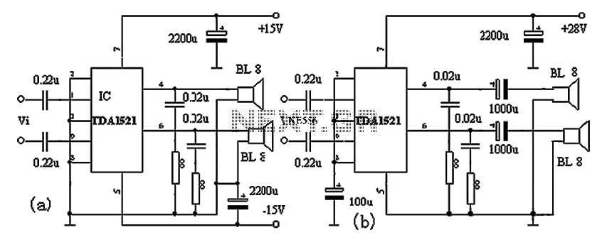
The TDA1521A amplifier circuit is designed for high-fidelity applications with minimal external components. It is suitable for powering Walkman devices or transforming low-powered computer speakers. The TDA1521A comes in a nine-pin single in-line plastic package and offers output power...
The digital scoreboard circuit is designed to display numerical values ranging from 0 to 9 on a common anode 7-segment display. The circuit employs a 7-segment driver integrated circuit (IC), specifically the 74LS47 or 74LS247. A 555 timer IC...