
astable multivibrator

The astable multivibrator circuit operates as a self-oscillating device, generating a square wave output without requiring any external triggering. The circuit typically consists of two transistors, resistors, and capacitors arranged in a feedback loop. In the correct configuration, the transistors are arranged in a complementary manner, allowing one transistor to turn on while the other turns off, creating a continuous oscillation.
The left circuit is characterized by its reliance on component tolerances and startup conditions. It may struggle to initiate oscillation due to insufficient feedback or improper timing in the charging and discharging of capacitors. In contrast, the right circuit's use of DC negative feedback enhances stability and reliability, ensuring that oscillation commences more readily. This is particularly beneficial in simulation environments where ideal conditions may not replicate real-world scenarios.
The capacitors in the circuit serve crucial roles in timing and feedback. C1, when charged, provides the necessary voltage to turn on Q1, while simultaneously influencing Q2's operation. The negative voltage at Q2's base during the discharge of C1 plays a pivotal role in the timing of the oscillation cycle. The interaction between C1 and C2, along with their respective resistors (R2, R3, R4), governs the frequency and duty cycle of the output waveform.
Protection measures, such as the inclusion of diodes in series with the emitters, are essential to safeguard the transistors from excessive reverse voltage, which could lead to failure. The careful selection of component values allows for the tuning of the oscillation frequency, making the astable multivibrator a versatile circuit for various applications, including clock pulses and signal generation in digital circuits.
In summary, the astable multivibrator's design, while simple, requires precise component selection and configuration to ensure reliable operation and effective performance in generating oscillations.The astable multivibrator I found in wikipedia and also my college material are the same, which is on the left hand side of the picture. While for the schematic at the right hand side, I found it from the example of LTSpice. I would say because it`s drawn wrongly, the correct circuit is the one on the left. It may perhaps work, but it`s not a go od example, and it`s not something I would consider. The circuit on the left is prone to not starting to oscillate, especially in simulations. The circuit on the right has DC negative feedback, which keeps the transistors out of saturation except right after they switch ON. This allows oscillation to start more readily, especially in simulations. There are ways of getting the circuit on the left to start in simulation. In practice, it will generally start, due to component mismatches and the startup transients introduced by the power supply turn-on step.
I agree that the circuit on the right is not as useful as the other one. Since the transistors don`t saturate, you won`t get good logic "0" levels, although there are relatively simple ways to get around this. The wire on the capacitor that connects to a transistor`s base is driven to a negative voltage when the other transistor conducts.
Then the capacitor discharges into R2. Since the max reverse voltage on a silicon transistor`s emitter-base junction is only about 5V then a small supply voltage is needed or protection diodes should be used in series with the emitters. When C1 is fully charged, Q1 is turned on. C1 acts as a battery and its -ve side is connected to the base of Q2, that`s why the potential at the base of Q2 is -ve when C1 starts discharging, right Then R3 charges or discharges C2 enough to turn on Q1 a little and the negative end of C1 drives the base of Q2 negative which turns off Q2.
Then both ends of C2 go positive which quickly turns on Q1 completely. Then C2 charges quickly into the base of Q1 through R4. At the same time, C1 is discharged slowly by R2 and when the voltage at the base of Q2 rises up to about +0. 6v then Q2 begins to turn on a little and the charge in C2 turns off Q1. 🔗 External reference
Related Circuits
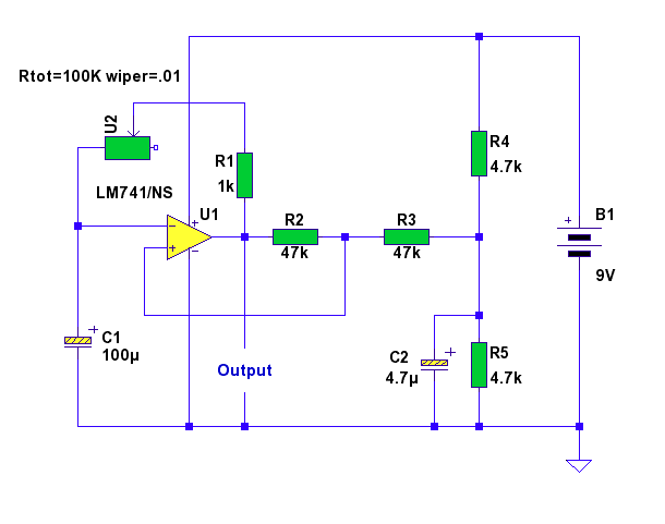
In this circuit, a standard operational amplifier (op-amp) is configured as an astable multivibrator. The output is non-symmetrical, but it has the advantage of being controlled by only one resistor and one capacitor: a 100k variable resistor (U2) and...
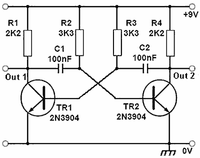
The basic bipolar transistor (BJT) version of an astable multivibrator has two outputs that repeatedly change state at a rate determined by the time constants of its feedback network. Although largely superseded by its equivalent op-amp or timer IC...

The 555 is a highly stable device for generating accurate time delays or oscillation. Additional terminals are provided for triggering or resetting if desired. In the time delay (monostable) mode of operation, the time is precisely controlled by one...

This plugin features a single 555 timer in astable mode. It is highly versatile and can be utilized for various applications, commonly serving as a clock signal generator for circuits. The configuration described produces a pulse frequency of approximately...
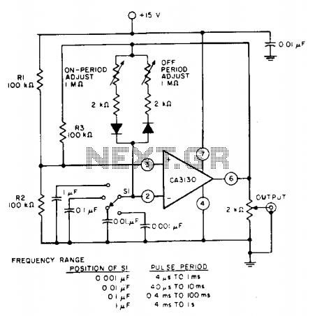
The pulse repetition rate is determined by adjusting switch SI to the desired position, and this rate remains relatively constant even when the resistors that control the on-period and off-period are modified. Resistors R1 and R2 set the biasing...
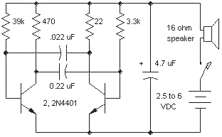
The astable flip-flop circuit is a versatile configuration used for creating flashers or generating square waves. A common application is an alternating LED flasher where the LEDs are connected in the emitters instead of the collectors, which is the...