
BJT Astable Multivibrators
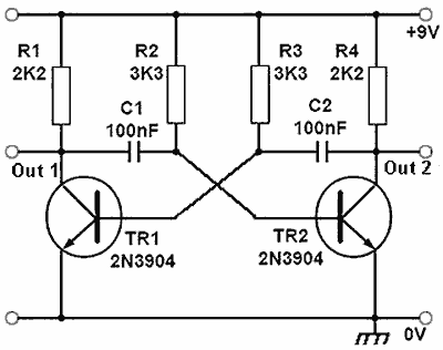
The bipolar junction transistor (BJT) astable multivibrator circuit operates as a fundamental oscillator, producing two complementary square wave outputs. The configuration consists of two NPN transistors (TR1 and TR2), resistors (R2, R3, R4, R5, and R6), and capacitors (C1 and C2) forming a feedback network that dictates the timing characteristics of the oscillation.
Upon powering the circuit, TR1 is initially in a conductive state, causing TR2 to remain off. The charging of capacitor C1 through resistor R2 establishes the initial conditions for oscillation. As C1 charges to approximately 0.6V, TR2 turns on, which causes a cascade effect that turns off TR1. This rapid switching action is responsible for generating the square wave outputs at the collectors of both transistors.
The timing of the oscillation is influenced by the values of the resistors and capacitors in the circuit. The time constants, determined by the products of resistance and capacitance (RC), govern the charging and discharging cycles of the capacitors, thus controlling the frequency of oscillation. The frequency can be expressed mathematically, allowing for precise design adjustments to achieve desired output characteristics.
In the modified version of the circuit, the introduction of diode D2 enhances performance by preventing the feedback capacitor C2 from affecting the operation of TR2 during its off state. This modification significantly improves the rise and fall times of the output waveforms, resulting in a more defined square wave signal. The ability to adjust the mark-to-space ratio through VR1 further adds to the versatility of the design, making it suitable for various applications in signal generation and timing circuits.
Overall, the BJT astable multivibrator remains a valuable circuit design, providing a cost-effective and efficient means of generating square waves and pulses in electronic applications.The basic bipolar transistor (BJT) version of an astable multivibrator as shown in Fig. 4. 1. 1 has two outputs that repeatedly change state at a rate determined by the time constants of its feedback network. Although largely superseded by its equivalent op amp or timer IC versions in many applications, it is still a useful and flexible design for s
quare wave and pulse generation. The circuit switches continuously from one state (TR1 on and TR2 off) to the other (TR1 off and TR2 on) and back again at a rate determined by the RC timing components Cl/R2 and C2/R3. The circuit produces two anti-phase square wave signals, with an amplitude almost equal to its supply voltage, at its two transistor collectors as shown in Fig 4.
1. 2. Suppose that at switch on, TR1 is conducting heavily and TR2 is turned off. The collector of TR1 will be almost at zero volts as will the left hand plate of C1. Beause TR2 is turned off at this time, its collector will be at supply voltage and its base will be at almost zero potential, the same as TR1 collector, because C1 is still un-charged and its two plates are at the same potential. C1 now begins to charge via R2 and its right hand plate becomes increasingly positive until it reaches a voltage of about +0.
6V. As this plate of the capacitor is also connected to the base of TR2, this transistor will begin to conduct heavily. The rapidly increasing collector current through TR2 now causes a voltage drop across R4, and TR2 collector voltage falls, causing the right hand plate of C2 to fall rapidly in potential.
It is the nature of a capacitor that when the voltage on one plate changes rapidly, the other plate also undergoes a similar rapid change, therefore as the right hand plate of C2 falls rapidly from supply voltage to almost zero, the left hand plate must fall in voltage by a similar amount. With TR1 conducting, its base would have been about 0. 6V, so as TR2 conducts TR1 base falls to 0. 6 ’9V = ’8. 4V, a negative voltage almost equal and opposite to that of the +9V supply voltage. This rapidly turns off TR1 causing a rapid rise in its collector voltage. Because a sudden voltage change on one plate of a capacitor causes the other plate to change by a similar amount, this sudden rise at TR1 collector is transmitted via C1 to TR2 base causing TR2 to rapidly turn on as TR1 turns off.
A change of state has occurred at both outputs. This new state does not last however. C2 now begins to charge via R3, and once the voltage on the left hand plate (TR1 base) reaches about +0. 6V another rapid change of state takes place. This switching action produces the collector and base waveforms shown in Fig. 4. 1. 3. The circuit keeps on changing state in this manner producing a square wave at each collector. The frequency of oscillation can be calculated, as the time for the relevant capacitor to charge sufficiently for a change of state to take place, will be approximately 0.
7CR and, as two changes of state occur in each cycle the periodic time T will be: A problem with the basic astable circuit is that the capacitor action described above slows down the rise in voltage as each transistor turns off, producing the curved rising edges to the square wave as can be seen in Fig. 4. 1. 2. This can be overcome by the modified circuit shown in Fig. 4. 1. 4 Each time TR2 collector voltage goes high as the transistor turns off, D2 becomes reverse biased, isolating TR2 from the effect of C2 charging.
The charging current for C2 is now supplied by R5 instead of R6. The action of TR1 during its off` period is similar. The output waveforms at the collectors of TR1 and TR2 shown in Fig. 4. 1. 5 demonstrate the improved rise times achieved by the modified circuit of Fig. 4. 1. 4, compared with those for the basic BJT astable circuit shown in Fig. 4. 1. 2. By varying VR1 the voltage at the top of both R3 and R4 is varied so that whatever mark to space ratio is used 🔗 External reference
Related Circuits

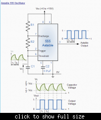
The 555 is a highly stable device for generating accurate time delays or oscillation. Additional terminals are provided for triggering or resetting if desired. In the time delay (monostable) mode of operation, the time is precisely controlled by one...
Simulation schematic for an astable multivibrator. Parameters: Vcc = 24V, Vol = 1V, Voh = 21V. The power supply is Vcc, with connections from Vcc to ground. The time constant is determined by R1 and the capacitor C1, where...
In the following astable multivibrator circuit, some sources state that the duty cycle is represented as d = (R1 + R2) / (R1 + 2 * R2), while other sources provide different information. The astable multivibrator circuit is a type...
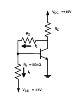
A circuit diagram has been provided for analysis, with the objective of calculating the values of resistors R2 and RC. The circuit is designed to operate at the Q-point with the following parameters: VCE = 5V, VBE = 0.7V,...
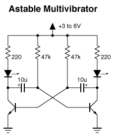
Two 47k ohm resistors, with alternative values ranging from 22k to 100k ohm, can be used. The value of these resistors affects the timing of the blinking; larger values result in slower blinking. In a typical electronic circuit designed for...

An astable multivibrator can be designed using a 555 timer IC, operational amplifiers, or transistors. The 555 timer IC provides accurate time delays ranging from milliseconds to hours, with the frequency of oscillation adjustable through simple modifications. This is...