
ATmega8 breadboard circuit Tutorial
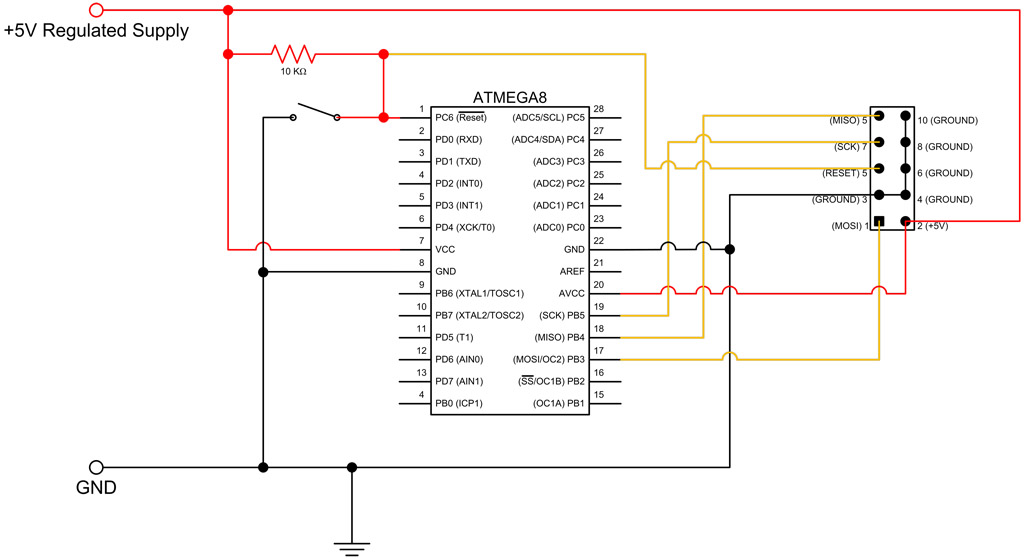
The microcontroller must be inserted onto the breadboard, requiring slight bending of the pins. One approach is to insert one side of the IC partially and bend the pins on the opposite side to fit into the corresponding tie points. Power must then be supplied to the IC. The ATmega8 has two ground pins (8 & 22), a VCC pin (7) for the positive power supply, and an analog VCC pin (20) to power the AD converter. During normal operation, pin 1 (PD0/Reset) should remain high. When this pin is grounded temporarily, it resets the system, as indicated by a horizontal line above the RESET label in the pinout diagram. This notation signifies that the function activates when the pin is grounded. A circuit comprising a 10kΩ resistor and a push button switch will be constructed. The resistor pulls the pin high for normal operation, while the pushbutton switch temporarily grounds the pin for the reset function. Without the resistor, pressing the pushbutton would divert all power to ground, resulting in no power for VCC/AVCC and potentially damaging the power supply. A micro tactile switch will be utilized, which has two pairs of pins, with each pair connected to each other. Straightening the pins on the micro tactile switch before inserting it into the breadboard is advisable.
The final step involves building the ISP (In System Programming) interface, which allows firmware to be written to the microcontroller using a programmer such as the USBASP AVR Programmer. The ISP interface will use a 10-pin IDC connector (shrouded/box header), which presents a challenge since these connectors do not fit on a breadboard due to the 0.1" (2.54mm) row spacing. The rows must be 0.3" (7.62mm) apart to fit on either side of the breadboard's center channel. One solution involves bending the pins of an IDC connector with right-angle leads, which, while not aesthetically pleasing, is functional. The IDC connector is then inserted and wired to the 5V supply, ground, and the microcontroller. Care should be taken when inserting the IDC connector, as its pins are thicker than the typical wires used in a breadboard setup.
The circuit design incorporates the necessary components and connections to create a functional microcontroller interface. The ATmega8 is powered correctly, with provisions for reset functionality and programming capability. The inclusion of the ISP interface ensures that firmware updates can be performed efficiently, making this setup suitable for various applications in embedded systems.This tutorial continues on from ATmega8 Breadboard Circuit Part 1 where we build a small power supply on the breadboard. In this part we will add the ATmega8 microcontroller and an interface to allow it to be programmed. The first step is to orient yourself with the ATMEGA8 microcontroller. Since we are building our circuit on a breadboard, we `re using the PDIP variant ( ATMEGA8-16PU ). You could also build this circuit using an ATmega48, 88, 168 or 328 as these all share the same pin layout but have slightly different features, clock speeds and memory. When you look at the microcontroller you will see a few makings which help identify the pin numbers. At one end there is a semicircle/half moon section. This denotes the top of the IC (Integrated Circuit). In a PDIP/DIP package the pins are numbered from 1 in an anticlockwise fashion from this marker. Additionally, on the ATmega8 there is a small circle identifying pin 1. When you look at the pin-out, you will notice that many of the pins are marked as I/O ports. e. g. Pin 28 has the label PC5 , which means Port C pin 5 . The I/O ports also have secondary functions which are noted in parenthesis. e. g. pin 28 has secondary functions of ADC5 (ADC Input Channel 5) and SCL (Two-wire Serial Bus Clock Line).
In some cases (e. g. reset on pin 1), the secondary function is much more commonly used than the primary function. Now it`s time to insert the microcontroller onto the breadboard. You will need to bend the pins inwards slightly. One method is to insert one side of the IC in shallowly then bend the pins on the other side so that they fit into the tie points on that side. You can then gently push/wiggle the IC in. Now we will supply power to the IC. The ATmega8 has 2 ground pins (8 & 22), a VCC pin (7) for positive power supply and an analog VCC pin (20) to provide power to the AD converter.
The figure below shows these connected up. For normal operation, pin 1 (PD0/Reset) needs to be kept high. When this pin is temporarily grounded, the system resets/reboots. This is indicated in the pinout diagram by the horizontal line above RESET . This notation is quite common and means the function is activated when the pin is grounded. We will build a circuit consisting or a 10k; resistor and a push button switch. The resistor pulls up the pin so that it is high for normal operation, whilst the pushbutton switch temporarily grounds the pin for the reset operation. If the resistor wasn`t there (i. e. replaced by a 0 ohm piece of wire), then pressing the pushbutton would divert all power to ground, which would mean no power for VCC/AVCC and blowing up the power supply.
The switch we are using is a micro tactile switch. These switches have 2 pairs of pins, with the pins in each pair connected to each other. This is shown in the diagrams below. You will find it useful to straighten the pins on the micro tactile switch prior to inserting it onto the breadboard. Now we just need to build the circuit onto the board. The last stage is to build the ISP (In System Programming) Interface. This allows for the firmware to be written to the microcontroller using a programmer, such as the USBASP AVR Programmer.
The ISP interface will be via a 10 pin IDC connector (shrouded/box header), which causes a problem for us. These connectors do not fit onto a breadboard because the rows are 0. 1 (2. 54mm) apart. We need the rows to be 0. 3 (7. 62mm) in order for them to fit on either side of the breadboard center channel. There are many solutions to this problem. We will be bending the pins on a IDC connector with Right angle leads. This may not look pretty, but it works. Lastly we insert the IDC connector then wire it up to 5V supply, ground and the microcontroller. Care must be taken when inserting the IDC connector, as the pins are a bit thicker that the wires you would normally insert into a breadboard.
i have a usbasp avr programmer, an 🔗 External reference
Related Circuits
It is said that mice are more sensitive to electromagnetic fields, which is why high-voltage grids generally yield poor results in rodent control. The electronic rodent control system described here does not use high-voltage power lines, thus it does...
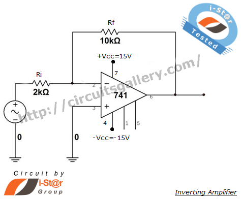
An inverting amplifier is one of the most widely used operational amplifier circuits. The output adjusts in a manner that counteracts changes caused by the input, thereby preventing saturation and ensuring stability. By connecting a resistor from the output...
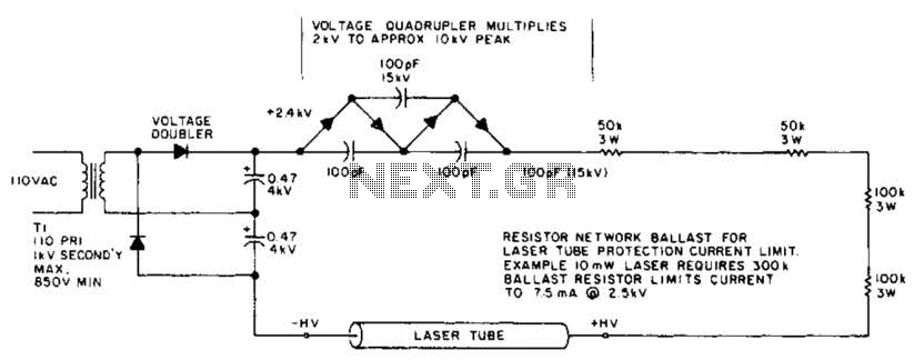
This circuit delivers a peak voltage of 10 kV, while limiting the current to 7.5 mA at 2 kV. The resistors included in the design serve the purpose of ballasting. Additionally, the starting circuit is unable to sustain the...
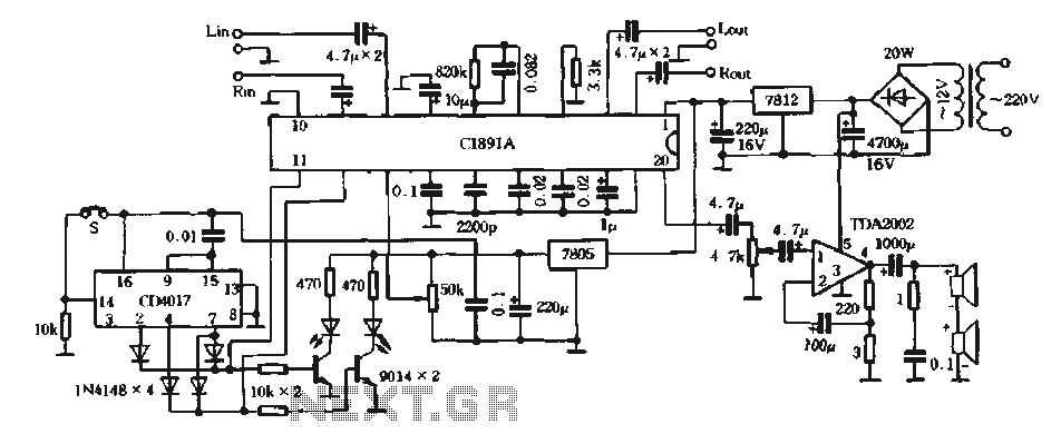
The surround processing section C1891A is a product from Sony Corporation of Japan that features a four-dimensional home theater surround processing circuit. It includes a parent roll phase-shifting circuit and a matrix surround sound amplifier. Additionally, it provides three...
This example describes the use of HS101 and HS201 radio transmitter and receiver modules to control rotating color lights, functioning as a multi-channel radio remote control device suitable for small dance floors or home use. Users positioned at any...

Lithium-based (Li+) batteries are increasingly used in portable devices due to their favorable characteristics. However, they are often in limited supply, leading to long lead times unless a preferred-customer status is established with manufacturers. Consequently, a backup alternative to...
Warning: include(partials/cookie-banner.php): Failed to open stream: Permission denied in /var/www/html/nextgr/view-circuit.php on line 713
Warning: include(): Failed opening 'partials/cookie-banner.php' for inclusion (include_path='.:/usr/share/php') in /var/www/html/nextgr/view-circuit.php on line 713