
Audio Astable Multivibrator Using IC 555 Circuit

The 555 timer IC, configured in this manner, serves as a versatile component in pulse generation applications. The astable multivibrator configuration allows for the continuous generation of square wave signals, which can be utilized in various electronic applications such as clock pulses for digital circuits, tone generation in audio applications, and timing intervals in control systems.
In this circuit, the resistors R1 and R2 and the capacitor C1 determine the frequency and duty cycle of the output waveform. The values of R1 and R2 can be adjusted to modify the timing characteristics of the circuit. For instance, increasing R1 or R2 will lengthen the period of the output signal, thereby lowering the frequency. Conversely, reducing these resistance values will result in a higher frequency output.
The capacitor C1 plays a crucial role in defining the charge and discharge times, influencing the overall behavior of the multivibrator. The choice of C1 value also affects the stability and response time of the circuit. It is important to select components that are rated appropriately for the intended application, considering factors such as voltage ratings and tolerance.
The output from the 555 timer can be taken from pin 3, which provides a square wave signal suitable for driving other circuits or components. The versatility of the astable multivibrator configuration makes it an essential building block in various electronic designs, allowing for straightforward integration into larger systems requiring timed pulses or clock signals.This circuit diagram shows how a 555 timer IC is configured to perform as an astable multivibrator. An astable multivibrator is a timing circuit whose `low` and `high` states are each unstable. As such, the output of an astable multivibrator toggles between `low` and `high` continuously, in result generating a train of pulses. This circuit is ther efore conjointly known as a `pulse generator` circuit. In this circuit, capacitor C1 charges through R1 and R2, eventually building up enough voltage to trigger an interior comparator to toggle the output flip-flop. Once toggled, the flip-flop discharges C1 through R2 into pin 7, which is that the discharge pin. When C1`s voltage becomes low enough, another internal comparator is triggered to toggle the output flip-flop.
This once more|once more|another time|yet again|all over again} permits C1 to charge up through R1 and R2 and the cycle starts everywhere again. C1`s charge-up time t1 is given by: t1 = zero. 693(R1+R2)C1. C1`s discharge time t2 is given by: t2 = zero. 693(R2)C1. Thus, the overall period of one cycle is t1+t2 = zero. 693 C1(R1+2R2). The frequency f of the output wave is that the reciprocal of this period, and is therefore given by: f = 1.
44/(C1(R1+2R2), wherein f is in Hz if R1 and R2 are in megaohms and C1 is in microfarads. 🔗 External reference
Related Circuits
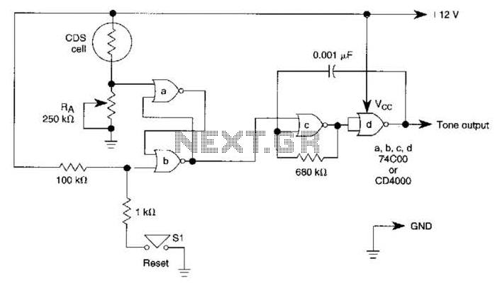
A decrease in the resistance of the CDS cell when light strikes it activates latch A and B, enabling tone oscillator C and D, which produces an output of about 1000 Hz. RA sets the trip level. SI resets...
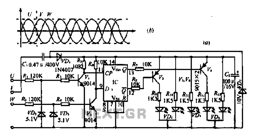
The three-phase voltage waveform diagram illustrates that when one phase voltage transitions from positive to negative across the zero point, the subsequent phase voltage becomes positive while the third phase remains negative. The U terminal voltage is positive when...
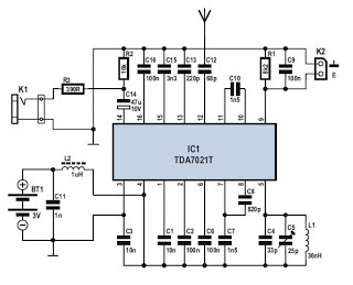
Several integrated circuits (ICs) are currently available that provide a nearly complete FM receiver solution. This project outlines a complete FM receiver circuit that offers excellent receiving and sound qualities. However, from a DIY enthusiast's perspective, the only drawback...
The Infrared IR Receiver circuit consists of a phototransistor, a microcontroller, and an amplifier. Understanding the data transfer between these three components is essential for successfully operating the circuit. The phototransistor receives digitally encoded data from an IR emitting...
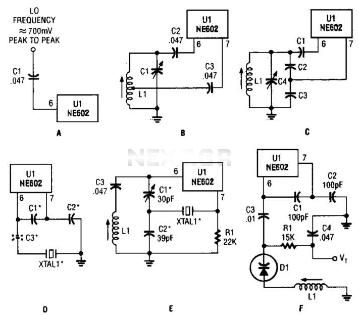
Any standard oscillator, such as a Colpitts or Hartley configuration, can be utilized to generate the local oscillator (LO) frequency required by the NE602. The NE602 is a versatile integrated circuit commonly used in radio frequency applications, particularly in mixer...
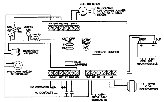
The following alarm circuit is designed with features that may be suitable for residential and commercial alarm system applications. It has a 12V and 1.5A regulated power supply. Furthermore, this residential alarm circuit also includes a delay circuit, a...