
Auto gain Control op-ampCircuit
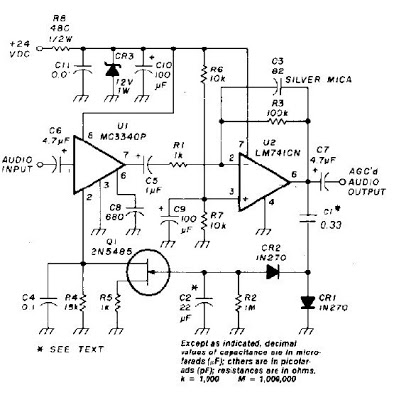
The circuit described operates as an automatic gain control (AGC) system, which is essential for maintaining a consistent audio output level in varying signal conditions. The operational amplifier (U2), specifically the 741 model, amplifies the incoming audio signal, which is then directed to a rectifier circuit comprised of diodes CR1 and CR2. This rectification process converts the AC audio signal into a negative DC voltage, which is critical for controlling the gate of the JFET (Q1).
Capacitor C1 plays a vital role in smoothing the rectified voltage, ensuring that the control voltage applied to the JFET is stable and free from high-frequency noise. The JFET operates as a variable resistor, with its resistance controlled by the gate voltage; as the negative voltage increases, the resistance of the JFET rises, effectively reducing the gain of the audio signal output from the MC3340P.
The MC3340P itself is a versatile audio attenuator that can adjust its gain based on the resistance connected to pin 2. The external resistor's value directly influences the gain, allowing for a range of adjustments from amplification to significant attenuation. The non-linear response of the gain relative to the external resistor is a characteristic feature of the circuit, which is common in many analog audio processing applications.
The combination of the JFET and the MC3340P ensures that the audio output remains consistent, even in the presence of fluctuating input signal levels. This AGC mechanism is crucial for applications such as broadcasting and audio recording, where maintaining a stable audio level is essential for quality sound reproduction. The design effectively integrates various components to achieve a reliable and efficient audio control system.An audio signal applied to VI is passed through the operational amplifier 741, U2. After being amplified, the output signal V2 is sampled and applied to a negative voltage doubler / rectifier circuit composed of diodes CRI and CR2, with the capacitor C1. The resulting negative voltage is used as a control voltage which is applied to the door] 2N54 85 FET Q1. Capacitor C2 and resistor R2 form a filter for smoothing the voltage rectified audio control. The lFET is connected between pin 2 of the MC3340P grounded by a resistor of 1 kohm. As the voltage applied to the gate of FET] becomes more negative in magnitude, the channel resistance of FET] increases causing lFET to function as a voltage-controlled resistor. The MC3340P audio attenuator is the heart of the MCO. It is capable of 13 dB of gain or almost - 80 dB of attenuation as a function of external resistor placed between Pin 2 and ground.
An increase in resistance decreases the gain from the MC3340P. The gain of the circuit is not entirely a linear function of the external resistance, but such behavior is similar across much of the gain / attenuation range. An input signal applied to the input of the AGC will cause the gate volt age the proportion lFET become negative.
Accordingly, the JFET increases the resistance of the pin 2 to ground the MC3340P causing a reduction in gain. In this way, the AGC output is kept almost constant. source by next. gr 🔗 External reference
Related Circuits

This is a speed motor controller circuit for a 12V DC motor. The speed of rotation of the spindle motor can be adjusted from 5 to 60 cycles per minute. The speed motor controller circuit for a 12V DC motor...
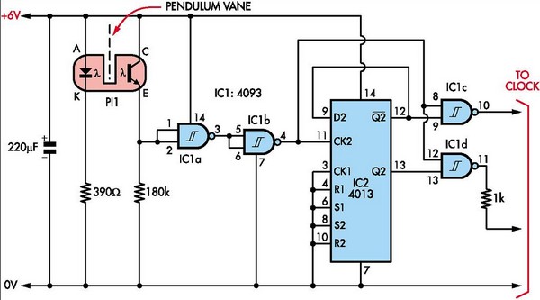
This document outlines the construction of a pendulum-controlled clock designed for high accuracy. Although it has a retro appeal, it represents an intriguing project. The project requires a spare quartz clock, which must be modified by isolating two pads...

A one-button control switch is designed to control two relays, each of which can switch the load power on and off as needed. The circuit primarily consists of a hex inverter CD4049 and two self-locking DC relays. The circuit utilizes...
Automatic Gain Control (AGC) is a circuit design that maintains a consistent level of amplification for sound or radio frequency signals. If the signal is too low, the AGC increases the gain to ensure the output remains at a...
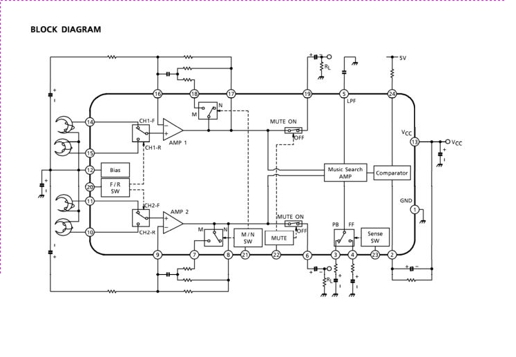
The TA2042F is a dual preamplifier with a music interval detection circuit designed for auto-reverse car stereo systems. This integrated circuit (IC) features dual amplifiers, a forward/reverse control switch, and a metal/normal tape equalizer. The TA2042F serves as a pivotal...
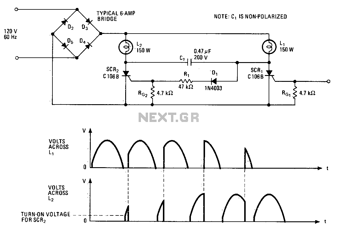
This lighting control unit will gradually decrease the brightness of one lamp while simultaneously increasing the brightness of another. The two loads maintain precise tracking without the need for manual adjustments. The gate of SCR1, a silicon-controlled rectifier, is...