
Automatic switch for batteries
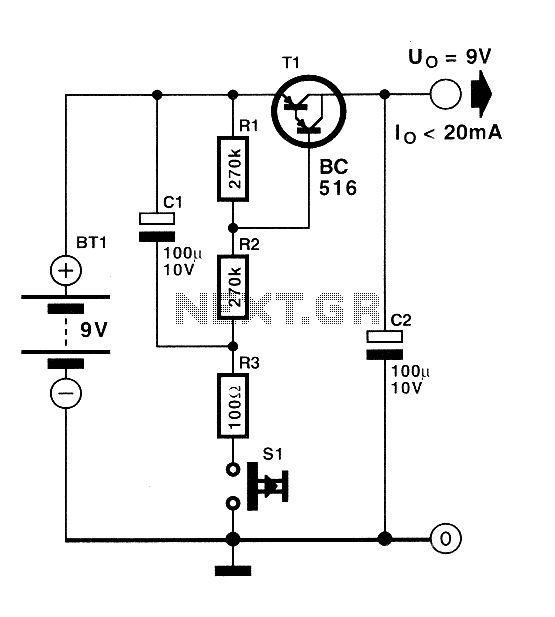
The circuit consists of a few components that can be integrated into any device powered by a 9V battery. Its primary feature is the ability to allow current to flow to the load for one minute upon pressing switch S1. After this duration, the circuit automatically disconnects the battery. The peak current during switching is 20 mA, which is adequate for most battery-operated devices at this nominal voltage. The core of the design is a PNP Darlington transistor (T1), which enters a conductive state when switch S1 is pressed. The small base current, facilitated by the transistor's high gain, allows it to remain in this conductive state even with relatively low capacitance values for capacitor C1 (approximately 100 µF). Resistor A3 limits the charging current to the capacitor, thus extending the duration for which the switch can be pressed. Resistors A1 and A2, along with capacitor C1, determine the time allowed for current to flow to the load. After this period, T1 is switched off, a condition ensured by resistor R1. In this design, the inclusion of a diode for reverse polarity protection is deemed unnecessary, as the maximum reverse voltage that the Darlington transistor can tolerate between the base and emitter (UBE) is 10V.
The circuit's architecture is designed for efficiency and simplicity, making it suitable for a variety of applications. It effectively manages power consumption by utilizing a timed current delivery mechanism. The PNP Darlington transistor serves as a reliable switch, allowing for a controlled discharge of the battery while preventing over-expenditure of energy. The use of resistors to regulate current flow and capacitor charge time is critical in ensuring the longevity of the battery's operational life. This design can be particularly beneficial in devices where battery replacement is inconvenient or where prolonged usage is essential. Overall, this circuit exemplifies an effective approach to managing battery life in portable electronic devices, emphasizing the importance of minimizing power consumption in the face of inevitable battery drain.Nowadays the batteries are gaining more and more power, being the only components that fail to provide energy for portable electronic devices. The evolution is rapid, leading manufacturers electronic equipment to attempt to minimize the consumption of their products so that they can operate for several hours using simple batteries trade.
In spite of the efforts of manufacturers, the device will absorb a zero power not yet invented. Thus, both small and if the current device is mathematically certain that at some point, after a few hours, days or ethdomades, the battery-drain '. The purpose of the circuit will describe below, is to keep 'alive' batteries for the maximum time, minimizing unnecessary consumption.
Taking a brief look at the circuit, you notice that the few parts that are can be integrated into any device powered by a battery of 9 V. The main trait is that allows current to flow to the load for a minute, since you pressed the switch S1.
After this time automatically cuts off the battery connection. The peak current during switching is 20 mA, price satisfactory for most devices that work with batteries, this nominal voltage. The heart of the construction is a Darlington type transistor PNP (T1), which is driven in a state of conduction through the pressing switch S1.
The small current thaoio, which is due to the high rate of aid, makes able to remain in this condition even for relatively small values ??of the capacity of capacitor C 1 (Around 100 MF). The resistance A3 limits the charge current of the capacitor, thus ensuring long life pressing the switch.
Resistance A1 and A2, in conjunction with the capacitor C 1, determine the period allowed to flow, flow to the load. After this time, the T1 is driven in the state cutoff, a condition ensured by R1. In this design, the placement of a diode to protect from any reverse polarity would be an unnecessary luxury, since the maximum reverse voltage that can accept darlington between thasis and emitter (UBE) is equal to 1O V.
🔗 External reference
Related Circuits
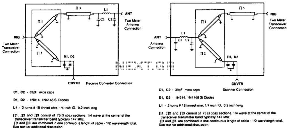
A pair of diodes and a quarter-wave transmission line are utilized as an automatic TR switch. D1 and D2 conduct during transmit periods, short-circuiting the scanner input. In this mode, the quarter-wave line appears as an open circuit. In...
The circuit diagram presented is a highly sensitive wireless relay switch designed to control home appliances such as flush systems and hand dryers. This wireless switch operates without the need for a remote control. It functions by simply moving...
The strategy involves assembling the circuit in stages, testing each component as it is integrated. Once all connections are established and can be controlled or read correctly by the computer, the main program can be developed with assurance that...
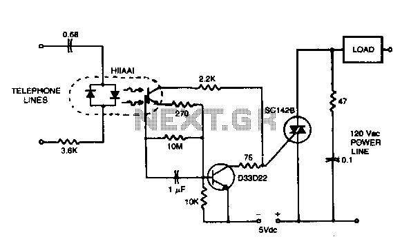
The circuit can operate lamps and buzzers from the 120 V, 60 Hz power line while maintaining positive isolation between the telephone line and the power line. The use of the isolated tab triac simplifies heat sinking by removing...

The audio-controlled switch utilizes a pair of 741 operational amplifiers, two 2N2222 general-purpose transistors, a hexFET, and several supporting components to create a circuit capable of activating devices such as a tape recorder, a transmitter, or virtually any other...
After turning off TT2, the input signal enters through chi Az, where the input resistance is very high and reaches the same potential. The inverting input terminal must also be associated with this movement. Therefore, Trr functions as a...