
BALANCED MODULATOR
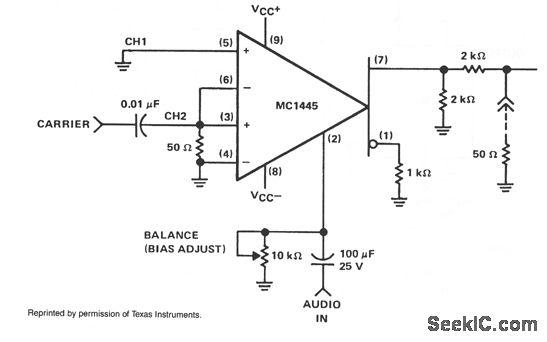
In this electronic circuit, the MC1445 modulator is employed to facilitate the modulation of signals using a carrier frequency. The cross-coupled differential amplifiers play a crucial role in this modulation process, enabling the switching of the modulation signal at the carrier rate. This is essential for applications requiring precise signal modulation, such as in communication systems.
The modulation signal's switching is influenced by the carrier level, which must be adequately set to ensure effective operation of the differential amplifiers. The symmetrical switching function generated during the modulation process is important for maintaining signal integrity. If the gate operates within the linear region, it ensures that only the first harmonic component is present, which is critical for reducing unwanted distortions in the output signal.
To balance the performance of the MC1445 modulator, it is vital to achieve equal gain across both channels. This balancing act is essential for maintaining signal fidelity and ensuring that the modulation characteristics remain consistent. The limitation of the modulation input to approximately 200 mV peak-to-peak is a design consideration that helps keep the system operating within the linear region, thus preventing distortion.
The sensitivity of the gate bias point to carrier suppression highlights the necessity for precise adjustments in the circuit. The use of a high-resolution, 10-turn potentiometer allows for fine-tuning of the bias point, ensuring optimal performance and stability of the modulation process. This attention to detail in component selection and circuit design is crucial for achieving reliable operation in various electronic applications.When the carrier level is adequate to switch the cross-coupled pair of differential amplifiers, the modulation signal, which has been applied to the gate, will be switched at the carrier rate, between the collector loads. When switching occurs, it will result in the modulation being multiplied by a symmetrical switching function.
If the modulation gate remains in the linear region, only the first harmonic will be present. To balance the MC1445 modulator, equal gain must be achieved in the two separate channels. To remain in the linear region, the modulation input must be restricted to approximately 200 mV pk-pk. Because the gate bias point is sensitive to the amount of carrier suppression, a high-resolution, 10-turn potentiometer should be used.
🔗 External reference
Related Circuits
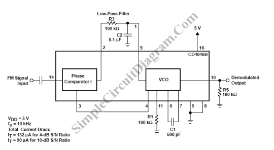
A Phase Locked Loop (PLL) can be utilized to create a Frequency Modulation (FM) demodulator. The PLL circuit tracks the input frequency by adjusting the voltage input of a Voltage-Controlled Oscillator (VCO). The Phase Locked Loop (PLL) is a critical...
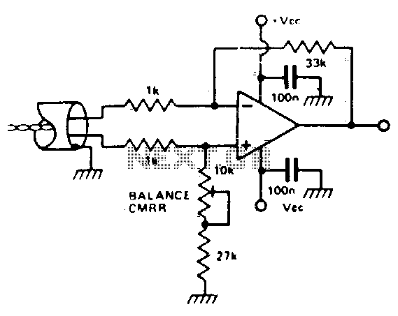
It is possible to simulate the balanced performance of a transformer electronically using a different amplifier. By adjusting the presets, the resistor ratio can be balanced to achieve the best Common Mode Rejection Ratio (CMRR). This method can yield...
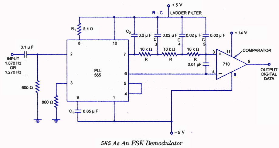
A highly effective application of the 565 Phase-Locked Loop (PLL) is its use as a Frequency Shift Keying (FSK) demodulator. In the 565 PLL, frequency shifting is typically achieved by driving a Voltage-Controlled Oscillator (VCO) with a binary data...
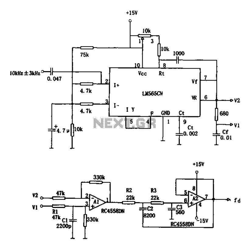
The circuit utilizes a 10 kHz and 3 kHz LM565CN to create an FM demodulation setup. The output diagram (b) illustrates the differential demodulation outputs V1 and V2 from the differential amplifier A1, which provides level displacement and amplification....
The circuit schematic of the UDC consists solely of dispersive components. Two low-frequency series LC resonators, with equal inductances (LA=LB) and capacitances (CA=CB), are connected to two input semi-infinite transmission lines, designated as A and B. These resonators are...
Here is a design circuit for a frequency modulator that is equipped with a tuning circuit. In this circuit, a pair of 1N4007 diodes is utilized as varactor diodes. The choice of 1N4007 diodes is not due to their...