
Frequency Modulator and Tuning Circuit
The frequency modulator circuit utilizes a pair of 1N4007 diodes configured as varactor diodes, which are essential for voltage-controlled capacitance. In this application, one varactor is directly connected to the crystal oscillator circuit through a 1 nF capacitor, allowing for significant changes in capacitance to influence the oscillator frequency. This direct coupling ensures that the frequency modulation is responsive and effective, as the capacitance variation directly affects the oscillation frequency.
The second varactor is coupled through a small trimmer capacitor, which enables precise adjustments to maximize its effect on the modulation process. This dual-channel approach allows for a coarse tuning mechanism alongside a fine-tuning option, facilitating both broad frequency adjustments and more delicate frequency-shift keying (FSK) modulation.
The overall design results in a frequency modulation output that can be characterized by a parabolic response curve, which is typical for such circuits. The parabolic nature of the data indicates the relationship between reverse voltage applied to the varactor diodes and the resulting frequency changes. However, it is important to note that any anomalies in the data, particularly in the fine-tuning trace, may arise from measurement errors, emphasizing the need for careful calibration and measurement techniques.
In summary, this frequency modulator circuit effectively employs varactor diodes to achieve tunable frequency modulation, with a robust design that allows for both coarse and fine adjustments, suitable for various applications in communication systems where frequency stability and modulation accuracy are paramount.Here`s a design circuit for frequency modulator that is completed with tuning circuit. In this circuit is using pair of 1N4007s are used as varactor diodes. I picked 1N4007s not because they are particularly well suited, but simply that I had some on the bench. One of the varactors is directly coupled to the xtal circuit through 1 nF so most of it s capacitance change is seen, the other is coupled through a small trimmer to adjust its maximum effect. This gives two independent channels, one for relatively coarse frequency tuning, the other for FSK modulation.
Here`s the figure of the circuit; The data looks characteristically parabolic as expected. I suspect the oddness of the fine is measurement error. The y coordinates are in Hz relative to 10. 138000 MHz (x is reverse voltage) so it doesn`t take much error in measurement to make the fine trace look lumpy. 🔗 External reference
Related Circuits
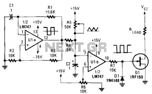
This circuit enables the effective power delivered to a load to be regulated by adjusting the duty cycle of the on/off ratio of the load current. The switching circuit does not dissipate any power. The operational amplifier U1A generates...
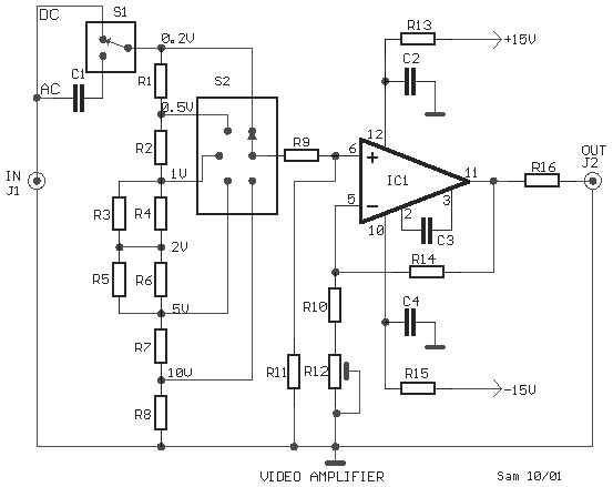
This is a schematic diagram of a video amplifier circuit, built using the very high-speed operational amplifier IC LH0032. Parts List: R1 = 15KΩ, R2, R3, R4 = 10KΩ, R5, R6, R7, R8, R9 = 1KΩ, R10 = 820Ω,...
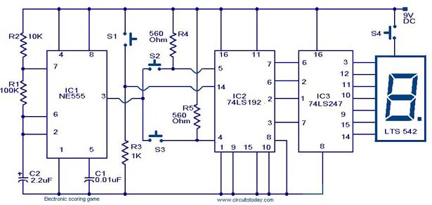
A scoring game circuit is explained with a circuit diagram and circuit parts. The scoring game circuit is designed to track and display scores in a gaming environment. The primary components of this circuit typically include a microcontroller, a score...
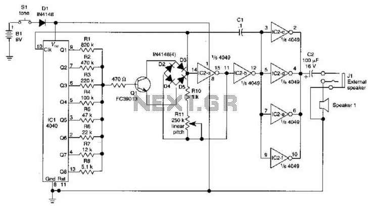
The circuit comprises four main components: a binary counter, a digital-to-analog (D/A) converter, a voltage-controlled oscillator (VCO), and an audio output amplifier. The counting speed of the binary counter is influenced by the frequency output from the VCO, which...
This amplifier is designed with the following specifications: distortion less than 0.1% at full power of 100W even at 20KHz, with power attributed to an extended bandwidth. The output transistors are protected against short circuits, and the power supply...
Schematic and description of a simple and easy-to-build NiCd and NiMH battery charger circuit that is capable of charging multiple NiCd and NiMH batteries. The circuit for the NiCd and NiMH battery charger is designed to be straightforward, allowing for...
Warning: include(partials/cookie-banner.php): Failed to open stream: Permission denied in /var/www/html/nextgr/view-circuit.php on line 713
Warning: include(): Failed opening 'partials/cookie-banner.php' for inclusion (include_path='.:/usr/share/php') in /var/www/html/nextgr/view-circuit.php on line 713