
basic cds photocell detector
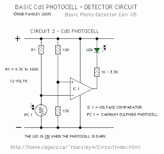
The basic Cadmium Sulfide (CdS) photocell detector circuit operates by utilizing the photoconductive properties of the CdS cell. When exposed to light, the resistance of the CdS photocell decreases, allowing more current to flow through the circuit. Conversely, when the light is obstructed, the resistance increases, leading to a higher voltage across the photocell. This voltage change is monitored by a comparator circuit, which is typically configured to compare the voltage across the photocell to a reference voltage set at half the supply voltage.
In practice, the selection of the resistor R1 is crucial for the proper functioning of the circuit. When installing the CdS photocell, it is essential to measure its resistance in the ambient lighting conditions to ensure accurate sensitivity settings. The recommended practice is to choose a resistor value that is three to five times greater than the measured resistance of the photocell. This approach allows for adequate sensitivity adjustments based on the specific application and environmental lighting conditions.
The output from the comparator can directly drive an LED, providing a visual indication of the light levels detected by the photocell. When the light level falls below a certain threshold, the comparator output switches to a high state, turning on the LED. This feature is particularly useful in applications such as automatic lighting systems, where the LED can signal the need for illumination in response to changing light conditions.
Overall, the design of the CdS photocell detector circuit highlights the importance of component selection and configuration to achieve the desired sensitivity and response characteristics. Adjustments to R1 can be made based on specific use cases, ensuring the circuit operates effectively across a range of lighting environments.This is a Basic Cadmium Sulfide (Cds) Photocell Detector circuit. In this circuit, when the light falling on the photocell (PC 1) is blocked, its resistance will increase and the voltage across PC 1 will rise. When the voltage rises above 1/2 of the supply voltage the output of the comparator will turn ON and the LED will be lit.
Due to wide varia tions in CdS photocells it is usually best to install the cell and then measure its resistance under normal lighting conditions. A resistor with a value that is approximately 3 to 5 times the measured resistance of the cell is then selected for R1.
For example; If the cell resistance is measured at 400 ohms then a 1200 to 2200 ohms resistor would be used. Increasing the value of R1 will cause the sensitivity of the sensor to decrease. This may be necessary when the light falling on the cell is not very strong or shadows can affect the photocell.
🔗 External reference
Related Circuits
A heat-sensitive sensor can be utilized to create a direction detector. This type of sensor responds to minimal heat. The specific sensor used in this design features a sensitive surface that has been divided into two sections. Consequently, it...
An A/D converter circuit can be represented by a simplified schematic, which illustrates a parallel type A/D converter. The term "median" refers to the number of bits in the digital signal output. The figure displays four A/D converters utilizing...
Similar to a field strength meter, an RF detector circuit serves as a valuable project for detecting nearby RF signals. The circuit presented here is capable of detecting a wide range of RF frequencies and provides an alarm when...
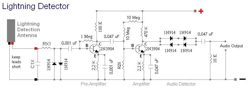
An audio amplifier connected to the output emits a loud click sound for each lightning strike detected. When severe storms approach, this receiver produces numerous clicks per minute. This is a direct detection amplified "crystal" radio receiver that does...
A circuit designed to detect the interruption of a light beam. The initial circuit was a light/dark detector using a photoresistor, which, while capable of detecting light interruptions, suffered from significant interference due to ambient light. This led to...
This circuit utilizes a 1458 dual operational amplifier (op-amp) to create a radar detector. Capacitor C1 serves as the sensor for the radar signal. The first op-amp is configured as a current-to-voltage converter, while the second op-amp functions as...