
basic circuit diagram for pc to microcontroller communication

The 8051 microcontroller's serial communication capabilities are essential for interfacing with various peripherals and devices. The TXD and RXD pins enable full-duplex communication, allowing simultaneous data transmission and reception. The TTL signal levels on these pins are suitable for direct connection to other TTL-compatible devices. However, for communication with RS232 devices, which operate at higher voltage levels, the MAX232 level shifter is employed. This IC converts the TTL signals to RS232 levels and vice versa, ensuring compatibility with standard serial communication protocols.
The Serial Control register (SCON) plays a critical role in configuring the serial communication modes. The bits SM0 and SM1 determine the mode of operation, which can be set to either 8-bit variable baud rate, 8-bit fixed baud rate, or 9-bit communication. The REN bit enables the reception of data, while TB8 and RB8 are used for 9-bit data transmission and reception, respectively. The TI and RI flags indicate the status of transmission and reception, allowing the microcontroller to manage data flow effectively.
In addition to serial communication, the 8051 microcontroller utilizes timer registers (TMOD and TCON) to control timing operations. The TMOD register defines the mode of operation for the timers, while the TCON register manages the timer's start, stop, and overflow conditions. This combination of serial communication and timer functionality allows the 8051 to perform complex tasks in embedded systems, making it a versatile choice for various applications.8051 provides a transmit channel and a receive channel of serial communication. The transmit data pin (TXD) is specified at P3. 1, and the receive data pin (RXD) is at P3. 0. The serial signals provided on these pins are TTL signal levels and must be boosted and inverted through a suitable converter(MAX232) to comply with RS232 standard. All modes a re controlled through SCON, the Serial CONtrol register. The SCON bits are defined as SM0, SM1, SM2, REN, TB8, RB8, TI, RI from MSB to LSB. The timers are controlled using TMOD, the Timer MODe register, and TCON, the Timer CONtrol register. 🔗 External reference
Related Circuits
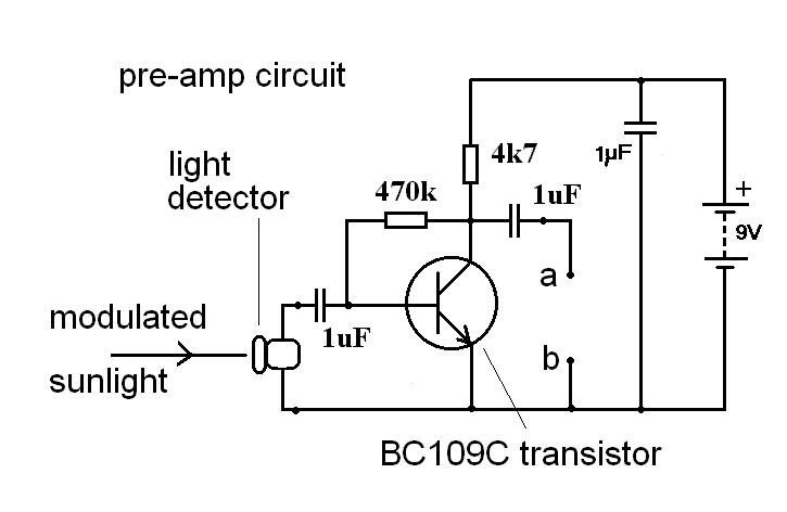
This document outlines a straightforward process to transmit voice over a distance using amplitude modulation of light through sound vibrations. It details how modulated light is detected and demodulated by a receiver to reproduce sound. The experiments described are...
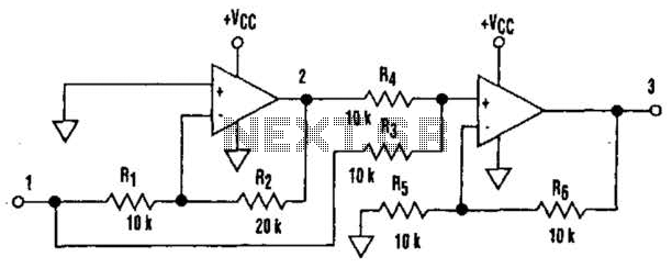
It is well understood that utilizing single-supply operational amplifiers (op amps) can present challenges when implementing simple functions in a bipolar signal environment. Often, this necessitates the use of additional op amps and other electronic components. Considering this, it...
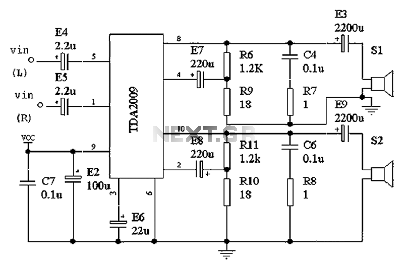
The intention was to develop a morning exercise machine, but the challenge was the absence of a suitable high-power amplifier. Since the exercise machine operates on battery power, the search for a solution persisted for several months. Eventually, the...

The motorcycle anti-theft alarm circuit consists of several components, including the anti-theft detection circuit, the control circuit, the sound generator, the audio oscillator, and the power amplifier output circuit, as illustrated in figure 7-91. The anti-theft detection circuit is...
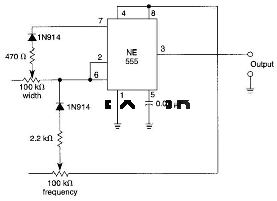
In this multivibrator circuit, frequency and pulse width can be separately controlled by using steering diodes (1N914) and two potentiometers. This multivibrator circuit utilizes steering diodes, specifically the 1N914 type, to enable independent control over both the frequency and pulse...
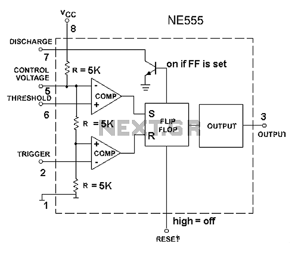
The 555 timer circuit, regardless of the manufacturer, has a consistent internal structure and performance. Various manufacturers produce different models of the 555 timer, including MC555, CA555, XR555, LM555, as well as domestic models like SL555, FX555, and 5G1555....