
Basic RF Oscillator

The basic RF oscillator circuit operates at a designated frequency of 7 MHz and is characterized by its simplicity and effectiveness. The primary component, TR1, acts as an emitter follower, providing a voltage gain close to unity, which is essential for maintaining signal integrity without excessive amplification. The use of two 27K resistors allows flexibility in component selection; these can be increased to 100K depending on the desired gain characteristics of the transistor used. For lower gain transistors, the 27K value is optimal.
Capacitors C2 and C3 are crucial in forming a voltage multiplier in conjunction with inductor L1, which is responsible for setting the oscillation frequency. The relationship between these components is critical, as C2 and C3’s values dictate the gain and overall performance of the oscillator. The design allows for a tuning capacitor of approximately 60 pF, which is achieved by combining C1, C2, and C3 in series. The ratios of C2 to C3 are typically set to 3:9, while C1 is varied between 1 to 10 times the wavelength to allow for fine adjustments in frequency.
The oscillator's functionality is enhanced by TR2, which serves as a buffer, isolating the oscillator from external loads and ensuring that the oscillation is not dampened by external circuitry. This configuration is vital for maintaining the stability of the oscillator's output.
For users looking to build the inductor L1, it is important to note that the construction method can significantly affect performance. Air-cored or ferrite core formers are recommended, with the acknowledgment that precise inductance values can vary based on the specific former used. The calculations for determining the required inductance based on capacitance values are essential for successful circuit operation.
Finally, the design emphasizes the importance of proper PCB layout for RF applications. Conventional breadboards and veroboards are inadequate for high-frequency circuits due to their poor grounding and signal integrity. Instead, high-quality PCBs with extensive copper planes for RF grounding are essential. These planes should cover as much area as possible to minimize resistance and inductance, ensuring optimal performance of the RF oscillator. Proper decoupling techniques must also be employed to maintain signal integrity and minimize noise in the circuit.Make a basic RF oscillator. The circuit is ridiculously simple, so I will skip all the complicated maths and make component selection simple by using calculators. Let us assume I want an oscillator for 7MHz. The circuit looks like this: The first transistor to the left (TR1) is a simple emitter-follower. It has a voltage gain of just under 1. The two 27K resistors can be as high as 100K, but if you want to use a lower gain transistor (2N2222 etc) then 27K is good. C2 and C3 work with L1 to form a voltage multiplier. The current is reduced, but TR1 is a current amplifier. In this way we have a total voltage/current gain of more than 1 between base and emitter. It will oscillate. TR2 (the other one) is a simple emitter follower that is used only as a buffer between the oscillator and the outside world. Here then are the brief specifications of the oscillator: I have included a few calculators here. Each time you see the text [Enter] you are being asked to enter data in the field. If you have previously used another calculator then there will already be default start values entered for you.
These are the results of your previous calculaton. You may of course enter new values. C1, C2 and C3 are all in series and so form a single tuning capacitor of about 60pf. The ratios of C2:C3 determine the gain and their values may vary quite a lot. In general, C2 = 3x wavelength, C3 = 9x wavelength. C1 can be any value from 1x wavelength to 10x wavelength and is normally chosen to fine-set the frequency of the oscillator. Make C1 start value about the same as C2. The actual values can vary over quite a wide range. This calculator will calculate the total tuning capacitance for your own selected values. In the above calculator, enter a frequency and click the "SHOW C1, C2 & C3" button and the values of C1, C2 & C3 will be displayed.
If you then click the "SHOW CAPACITANCE" button, you will see the value of the effective tuning capacitor that will be resonated with L1. You may also enter your own C1, C2 and C3 values to find the effective tuning capacitor that will be resonated with L1.
The inductor L1 resonates with the total capacitance above to determine the operating frequency. If you know the capacitance, having just read the the previous chapter, then use your basic frequency (transposed) to give inductance, or plonk your values in this little calculator: Now you know the inductance and the capacitance, it is just to buy and insert those values into the circuit. But if you really want to wind the coils yourself, then you will probably use either air-cored 6mm Dia.
formers, or use formers with a ferrite core. There are precise formulas to use but I like this method. Insert the required inductance and click the button. Please remember that this last "calculation" is very approximate since a lot depends upon the individual former. The "Ferrite core" is assumed to be a re-wound IF can as shown in the photos below. There are many types of construction one could use, but not all are any good. Veroboard, Breadboard and such commercial boards are almost useless for radio frequency work. Forget them! Printed Circuit Boards (PCBs) are great for RF, but there should be loads of supply decoupling connecting the +ve and -ve copper tracks together.
RF wiring is NOT like connecting a battery to a bulb (lamp). The "RF Earth" (ground) is usually the battery terminals and these copper planes should be as large as possible and cover as much area of the board as you can get. All other ptracks should be as short and thin as poss 🔗 External reference
Related Circuits
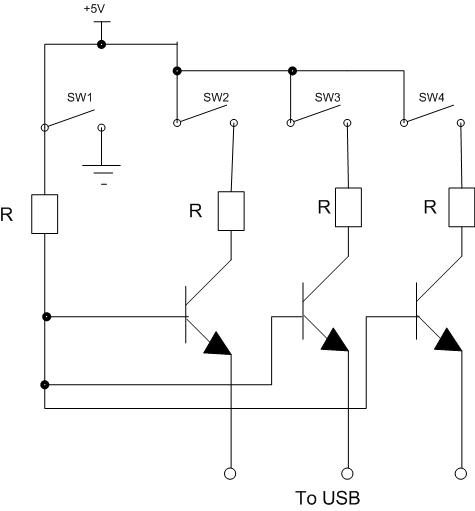
Four switches will be connected to a USB joystick board. The USB board has +5V and ground connections and emulates a button press. The circuit involves interfacing four mechanical switches with a USB joystick interface. The USB joystick board typically...
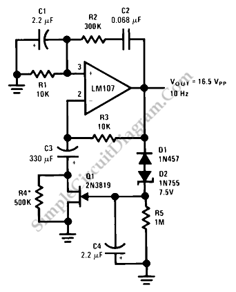
This is a sine wave oscillator circuit, also known as an amplitude-stabilized sine-wave oscillator. It can provide a high purity sine wave output. The sine wave oscillator circuit is designed to generate a stable and high-quality sine wave output, which...
The oscillator that consists of a quartz crystal can be classified into two types: the parallel resonant type crystal oscillator and the series resonant type crystal oscillator. The parallel resonant type crystal oscillator and its AC equivalent circuit are...
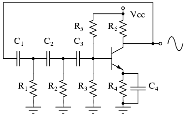
The phase shift oscillator produces a sine wave output in the audio frequency range. Resistive feedback from the collector results in negative feedback due to a 180-degree phase inversion from the base to the collector. The three 60-degree RC...
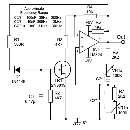
A basic Wien Bridge Oscillator utilizes a filament lamp in conjunction with an operational amplifier (op-amp). The property of filament lamps, specifically the non-linear increase in resistance of the tungsten filament as it heats, plays a crucial role in...
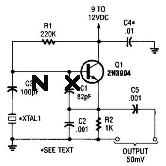
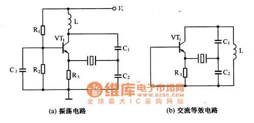
This is a simple Colpitts crystal oscillator for 1 to 20 MHz, which can be easily constructed from spare parts, provided that a crystal is available. The Colpitts oscillator is a type of electronic oscillator that utilizes a combination of...