
Basic single-supply voltage regulator
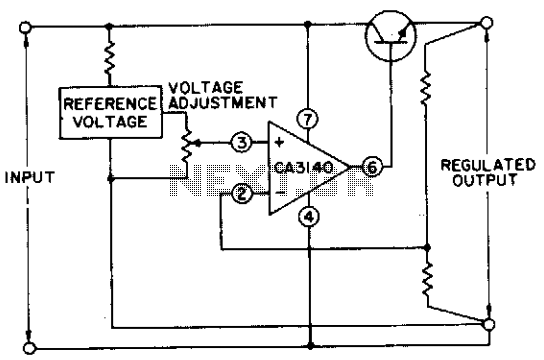
The CA3140 BiMOS operational amplifier is a versatile component that combines the advantages of both bipolar and CMOS technologies, resulting in high input impedance and low output impedance. This enables the op amp to function effectively in various applications, including power supply regulation.
In this circuit, the CA3140 is configured in a feedback loop to maintain a stable output voltage. The output voltage can be adjusted by varying the resistance in the feedback network, typically implemented using a potentiometer. This adjustment allows for a smooth transition across the entire range of 0 to 24 volts, making the circuit suitable for powering different electronic devices with varying voltage requirements.
The fully regulated nature of the circuit ensures that fluctuations in input voltage or load conditions do not significantly affect the output voltage. This is achieved through the op amp's feedback mechanism, which continuously monitors the output and adjusts the input accordingly to maintain the desired voltage level.
Additional components may include capacitors for stability and filtering, as well as protection diodes to prevent reverse polarity or overvoltage conditions that could damage the op amp or the load. Proper thermal management should also be considered, especially if the circuit is expected to deliver high current levels, as excessive heat can affect performance and reliability.
In summary, the circuit employing the CA3140 BiMOS op amp is designed to provide a reliable and adjustable voltage source, characterized by its full regulation capabilities, making it a valuable solution for a wide range of electronic applications.The circuit uses a CA3140 BiMOS op amp capable of supplying a regulated output that can be adjusted from essentially 0 to 24 volts. The circuit is fully regulated. 🔗 External reference
Related Circuits
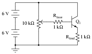
It is important to note that not all transistors have the same terminal designations or pinouts, despite having similar physical appearances. This distinction will influence how transistors are interconnected and connected to other components, making it essential to consult...
The project encompasses both hardware and software design for a 12/24V DC 20A charge controller suitable for solar, wind, hydro, or pedal power applications. This initiative aims to create an open-design, cost-effective, yet fully functional charge regulator for renewable...
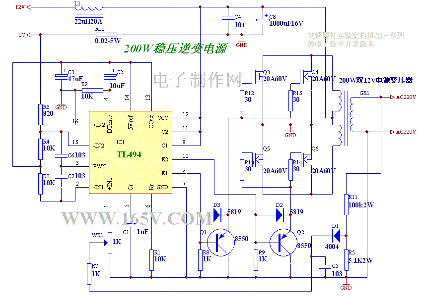
A stabilized voltage inverter that converts 12V to 220V with a power rating of 200W is illustrated in the accompanying diagram. This inverter can utilize an existing dual 12V-200W mains transformer; however, it exhibits low inverter efficiency. The described stabilized...
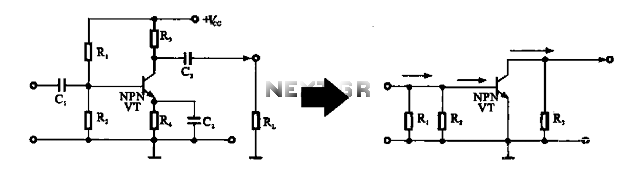
An alternating current voltage amplifier transistor AC path is described. In AC analysis, the internal resistance of the AC supply voltage source is low, which corresponds to a short circuit signal. Consequently, the alternating voltage terminal Vcc is considered...
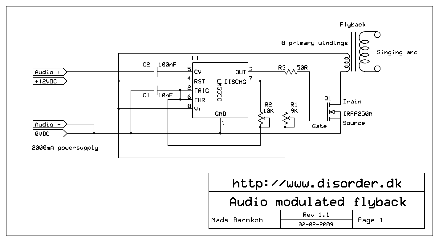
The iPod Shuffle has malfunctioned, likely due to a failure in the controller chip for the mini jack, resulting in the inability to detect the charger, PC connection, or headphones. The arc must be kept short to minimize distortions...
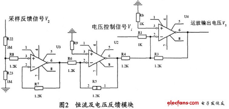
The output current range of the parameter current regulator is limited, and its precision is not high. Connecting the feedback adjustment type output current of the current-stabilized power source in series results in lower efficiency. The steady current source...