
Voltage follower
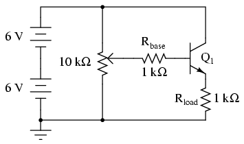
The voltage follower circuit is a fundamental configuration in analog electronics, primarily used for impedance matching. Its design typically includes a single bipolar junction transistor (BJT) configured in a common collector arrangement. The circuit's operation hinges on the transistor's ability to provide a high input impedance at the base and a low output impedance at the emitter, thus allowing the circuit to drive loads without significant voltage drop.
In practical applications, the voltage follower circuit is employed to buffer signals, ensuring that the voltage level remains consistent while allowing for increased current delivery to the load. This is particularly useful in interfacing between high-impedance sources and low-impedance loads, where signal integrity is paramount. The schematic representation of this circuit would typically include the BJT, power supply connections, and load resistor, alongside the necessary biasing resistors to establish the operating point of the transistor.
When assembling this circuit on a breadboard, the correct identification of the transistor terminals is crucial. The collector is connected to the power supply, the emitter to the load, and the base to the input signal source through a resistor. The load resistor is then connected to ground, completing the circuit. Testing should include measuring the input and output voltages as well as the currents to verify the expected performance characteristics, ensuring that the circuit operates within the desired parameters.Beware that not all transistors share the same terminal designations, or pinouts, even if they share the same physical appearance. This will dictate how you connect the transistorstogether and to other components, so be sure to check the manufacturer`s specifications (component datasheet), easily obtained from the manufacturer`s website.
Beware that it is possible for the transistor`s package and even the manufacturer`s datasheet to show incorrect terminal identification diagrams! Double-checking pin identities with your multimeter`s "diode check" function is highly recommended. For details on how to identify bipolar transistor terminals using a multimeter, consult chapter 4 of the Semiconductor volume (volume III) of this book series.
Again, beware that the transistor you select for this experiment may not have the same terminal designations shown here, and so the breadboard layout shown in the illustration may not be correct for you. In my illustrations, I show all TO-92 package transistors with terminals labeled "CBE": Collector, Base, and Emitter, from left to right.
This is correct for the model 2N2222 transistor and some others, but not for all; not even for all NPN-type transistors! As usual, check with the manufacturer for details on the particular component(s) you choose for a project.
With bipolar junction transistors, it is easy enough to verify terminal assignments with a multimeter. The voltage follower is the safest and easiest transistor amplifier circuit to build. Its purpose is to provide approximately the same voltage to a load as what is input to the amplifier, but at a much greater current.
In other words, it has no voltage gain, but it does have current gain. Note that the negative (-) side of the power supply is shown in the schematic diagram to be connected to ground, as indicated by the symbol in the lower-left corner of the diagram. This does not necessarily represent a connection to the actual earth. What it means is that this point in the circuit - and all points electrically common to it - constitute the default reference point for all voltage measurements in the circuit.
Since voltage is by necessity a quantity relative between two points, a "common" point of reference designated in a circuit gives us the ability to speak meaningfully of voltage at particular, single points in that circuit. For example, if I were to speak of voltage at the base of the transistor (VB), I would mean the voltage measured between the transistor`s base terminal and the negative side of the power supply (ground), with the red probe touching the base terminal and the black probe touching ground.
Normally, it is nonsense to speak of voltage at a single point, but having an implicit reference point for voltage measurements makes such statements meaningful: Build this circuit, and measure output voltage versus input voltage for several different potentiometer settings. Input voltage is the voltage at the potentiometer`s wiper (voltage between the wiper and circuit ground), while output voltage is the load resistor voltage (voltage across the load resistor, or emitter voltage: between emitter and circuit ground).
You should see a close correlation between these two voltages: one is just a little bit greater than the other (about 0. 6 volts or so ), but a change in the input voltage gives almost equal change in the output voltage. Because the relationship between input change and output change is almost 1:1, we say that the AC voltage gain of this amplifier is nearly 1.
Not very impressive, is it Now measure current through the base of the transistor (input current) versus current through the load resistor (output current). Before you break the circuit and insert your ammeter to take these measureme 🔗 External reference
Related Circuits
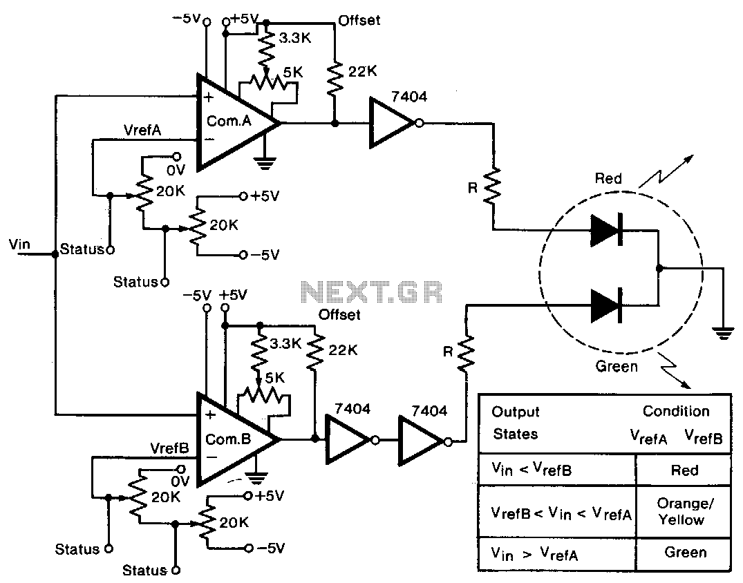
A tricolor LED serves as the visual indicator for voltage levels. The voltage to be measured is connected to two comparators in parallel. The first 20-KΩ trimmer sets a reference voltage between ±5 V, establishing the full-scale reference value....
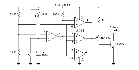
In this circuit, an LM339 quad voltage comparator is utilized to generate a time delay and control a high current output at low voltage. Approximately 5 amps of current can be sourced using a pair of fresh alkaline D...
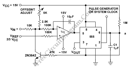
This is a circuit for a Voltage-to-Pulse Duration Converter. The circuit is designed to convert voltage into pulse duration by integrating a timer IC and an operational amplifier (OP Amp). The Voltage-to-Pulse Duration Converter circuit utilizes a timer IC, typically...
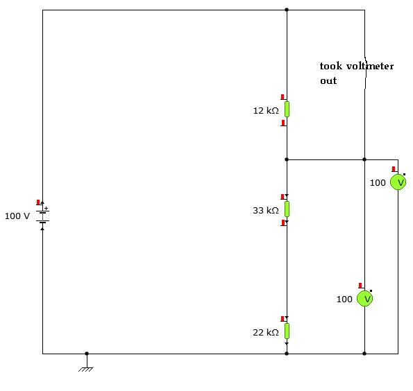
A user is utilizing YENKA software to diagram circuits but is experiencing confusion regarding the voltage calculations in a basic series circuit, as illustrated in the attached image. In a basic series circuit, components are connected end-to-end, forming a single...
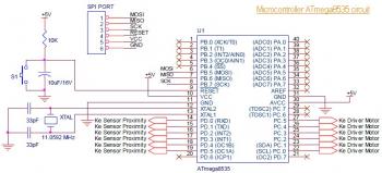
This is the circuit diagram of a line follower/line tracker robot. The circuit is derived from tutorial documentation, which can be downloaded at the end of this article. The line follower robot utilizes eight proximity sensor modules. Each sensor...
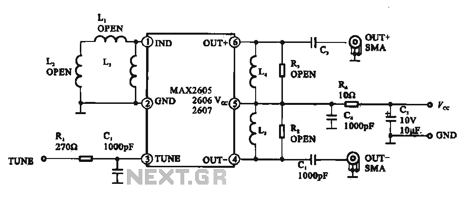
A low phase noise voltage-controlled oscillator circuit is presented, specifically integrated within the MAX2605-2609 voltage-controlled oscillator series. The circuit features a tuning voltage control terminal, allowing for adjustable oscillation frequency through a DC voltage input. The output of the...