
Basic Wide Range Phase Locked Loop (PLL)
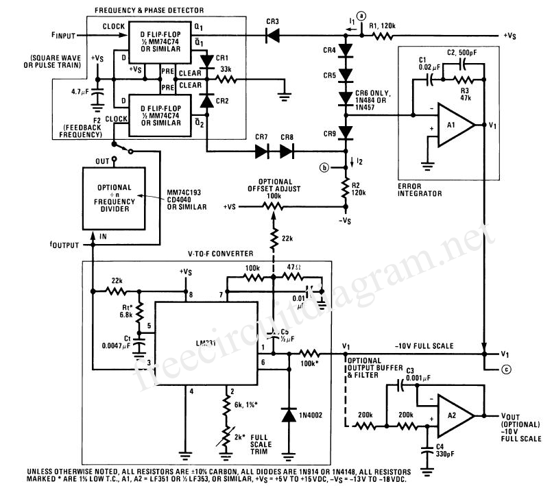
A phase-locked loop (PLL) serves as a critical component in various electronic systems, particularly in communication technologies where precision timing and frequency control are paramount. The described PLL configuration employs a dual-D flip-flop arrangement for phase and frequency detection, a departure from traditional quadrature detectors. This design choice not only simplifies the circuit but also enhances its cost-effectiveness and power efficiency.
The operation of the PLL begins with the clean input signal, which is essential for the system's performance. The dual-D flip-flops act as the core of the phase detection mechanism. When the input frequency (FIN) exceeds the reference frequency (F2), the first flip-flop (Q1) transitions to a high state, generating an error signal that is processed through the associated components (CR3 to CR6). This error signal is crucial for the integrator, which adjusts the control voltage to maintain phase alignment.
In scenarios where the input frequency matches the reference frequency, the relationship between the rising edges of both signals becomes critical. The phase difference is directly translated into the duty cycle of Q1, allowing for precise adjustments to be made. The PLL effectively maintains synchronization by minimizing the phase error to nearly zero, indicated by the generation of 30-nanosecond pulses from Q1 and Q2. These pulses ensure the system is reset for continuous operation, enabling the PLL to function efficiently over extended periods.
The choice of components, such as the MM74C74 flip-flop, is significant for this PLL design. Its lower power consumption and cost compared to alternatives make it suitable for applications requiring operation below 1 MHz. For applications where higher frequencies are necessary, the DM74S74 can be employed to achieve the desired performance with minimal delay, further enhancing the PLL's versatility.
Overall, this PLL design exemplifies an innovative approach to frequency and phase synchronization, with practical applications in modern communication systems where signal integrity and reliability are essential.A phase-locked-loop (PLL) is a servo system, or, in other words, a feedback loop that operates with frequencies and phases. PLL`s are well known to be quite useful (powerful, in fact) in communications systems, where they can pluck tiny signals out of large noises.
Here, however, we will discuss a new kind of PLL which cannot work with low-level s ignals immersed in noise, but has a new set of advantages, instead. It does require a clean noise-free input frequency such as a square wave or pulse train. Here is a schematic drawing: The basic circuit shown in Figure has all the functional blocks of a standard PLL. The frequency and phase detection do not consist of a quadrature detector, but of a standard dual-D flip-flop.
When the frequency input is larger than F2, Q1 will be forced high a majority of the time, and provide a positive error signal (via CR3, 4, 5, and 6) to the integrator. If F input and F2 are the same, but the rising edges of F input lead the rising edges of F2, the duty cycle of Q1=HI will be proportional to the phase error.
Thus, the error signal fed to the integrator will decrease to nearly zero, when the loop has achieved phase-lock, and the phase error between FIN and F2 is zero. Actually, in this condition, Q1 will put out 30 nanosecond positive pulses, at the same time that Q2 puts out 30 nanosecond negative pulses, and the net effect as seen by the integrator is zero net charge.
The 30 nanosecond pulses at Q1 and Q2 enable both flip-flops to be CLEARED, and prepared for the next cycle. This phase-detector action is substantially the same as that of an MC4044 Phase-Detector, but the MM74C74 is cheaper and uses less power.
It is fast enough for frequencies below 1 MHz. (At higher frequencies, a DM74S74 can be used similarly, with very low delays. ) We aim to transmit more information by carrying articles. Please send us an E-mail to wanghuali@hqew. net within 15 days if we are involved in the problems of article content, copyright or other problems. We will delete it soon. 🔗 External reference
Related Circuits
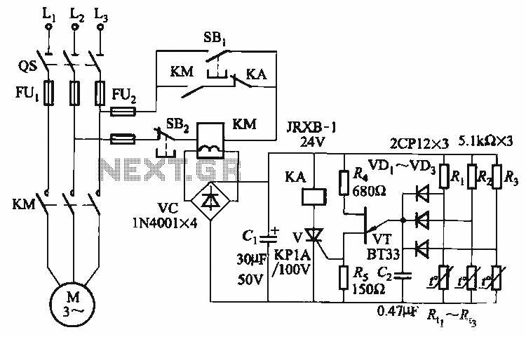
The thyristor control circuit includes a bridge circuit designed to regulate the temperature in the contactor coil KM, along with a secondary winding that functions as a power protection device. It comprises a thermistor (R:., Rt3) and a resistor...
Loop Antennas are considered to be small when their diameter drops below about 1/10 of the wavelength they are intended to be used at. In this case, the term "Tiny" is used because the antenna's diameter is about 1/30,000...
This circuit represents a basic version of a commercial uninterruptible power supply (UPS), providing a constant regulated output of 5 volts and an unregulated 12-volt supply. In case of a power failure, the battery seamlessly takes over, ensuring there...
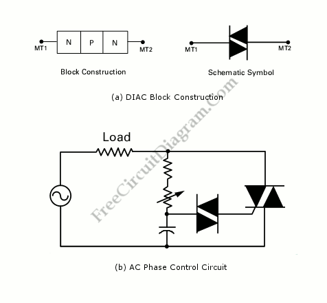
A diode for alternating current is a trigger diode that conducts current only after the DIAC reaches the breakdown voltage. The breakdown voltage of the DIAC is 30 V. A DIAC, or Diode for Alternating Current, is a semiconductor device...
The ADM1066 is a configurable supervisory and sequencing device that provides a single-chip solution for supply monitoring and sequencing in systems with multiple power supplies. In addition to these capabilities, the ADM1066 features a 12-bit ADC and six 8-bit...
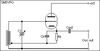
Observing the bottom of a valve reveals the wires connected to each electrode and the valve base pins. Therefore, specific valve data or pin-outs will not be provided, as this information is widely accessible from various sources, and most...