
Battery-Saving Disconnect Switch

The circuit is designed to protect the battery from over-discharge by disconnecting it from the load when the voltage drops to a critical level. The use of a high-side floating-source MOSFET (Q1) allows for efficient switching with minimal voltage drop across the device when it is in the ON state. The current consumption of the circuit is low, drawing only 500 µA during operation and reducing to 8 µA when idle, which helps to extend battery life.
The voltage thresholds, VU and VL, are determined by the resistors R1, R2, and R3, which form a voltage divider that monitors the battery voltage. The circuit requires that the input voltage (V+) exceeds a certain threshold (VO) for the voltage detector IC1 to activate IC2. This ensures that the circuit only operates when there is sufficient battery voltage available.
IC2, a dual charge-pump inverter, is responsible for generating a higher voltage for driving the gate of Q1. The charge-pump configuration, which includes capacitors (C1 and C2) and diodes, effectively multiplies the input voltage to create a gate drive voltage that can exceed the battery voltage, allowing Q1 to turn on fully.
The hysteresis implemented in the circuit, with a threshold difference of approximately 0.5 V between VL and VU, prevents rapid toggling of the switch during minor fluctuations in battery voltage. This feature ensures stability in the operation of the circuit, allowing it to disconnect at 3.1 V and only reconnect when the voltage recovers to 3.6 V.
The design also accounts for the ON-resistance of Q1, which increases as the battery voltage decreases. This is critical for maintaining efficient operation; even at the threshold voltage, the drop across the switch remains low (30 mV at 300 mA load), ensuring minimal energy loss. Resistor R4 plays a vital role in ensuring that Q1 turns off completely by providing a discharge path for C2, thus facilitating the proper operation of the circuit and enhancing its reliability. At a predetermined level of declining terminal voltage, the circuit disconnects the battery from the load and halts potentially destructive battery discharge. Ql, a high-side, floating-source MOSFET, acts as the switch. The overall circuit draws about 500 when the switch is closed and about 8 when it"s open. The values of ii, R2, and R3 set the upper and lower voltage thresholds, Vv and VL, according to the relationships For the circuit to start, V+ must exceed VO. The voltage detector IC1 then powers IC2, but only while V+ remains above VL. Otherwise, IC2 loses its power, removes gate drive from Ql, and turns it off. IC2 is a dual chaige-pump inverter that normally converts 5 V to + 10 V. Capacitors CI, C2, and the two associated diodes form a voltage tripler that generates a gate drive for Ql that is approximately equal to two times the battery voltage.
With the values in the schematic, the circuit disconnects 3-cell Nicad battery from its load when V+ reaches a VL of 3.1 V. Approximately 0.5 V of hysteresis prevents the switch from turning on immediately when the circuit removes the load; V+ must first return to Vu, which is 3.6 V.
The gate drive declines as the battery voltage declines, cause the ON-resistance of Ql to reach a maximum of approximately 0.1, just before V+ reaches its 3.1-V threshold. A 300-mA load current at that time will cause a 30-mV drop across the disconnect switch. The drop will be 2 to 3 mV less for higher battery voltages. Resistor R4 ensures that Ql can adequately turn off by providing a discharge path for C2. 🔗 External reference
Related Circuits
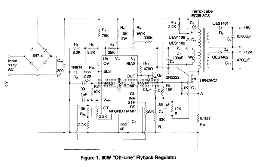
This paper gives a practical example of the design of an off-line switching power supply. Factors governing the choice of a discontinuous flyback topology are discussed. The design uses a pulsed-width modulation (PWM) control scheme implemented with a Unitrode...
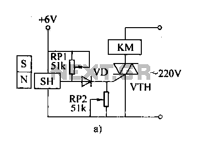
The automatic weapon features a magnetic switch circuit that is simple, reliable, has a low failure rate, and offers good versatility. It can be used for output performance or converted into mechanical displacement applications. The circuit diagram utilizes a...
The modern mechanic switches are improved concerning old technology. We need, however, many times to replace some old switch or to check currents bigger than the durability of certain switches or simply we need something with a modern appearance....
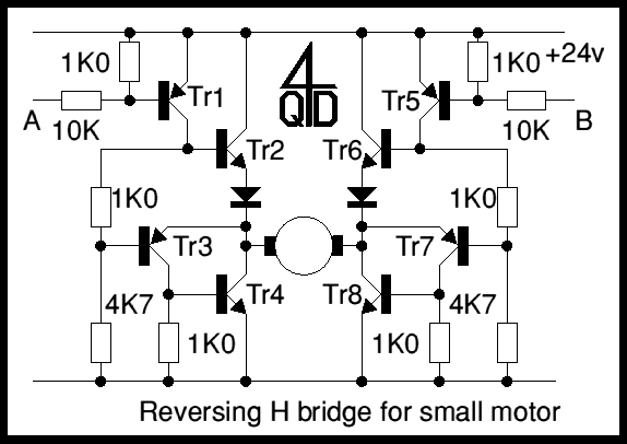
4QD manufactures motor speed controllers, and all their H bridges utilize PWM. This is a simple switch circuit designed for reversing and stopping a motor without speed control. Two inputs, A and B, control the bridge. When both inputs...
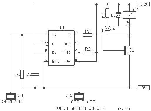
This is a touch switch designed to control LEDs, relays, and similar devices through a buffer transistor stage. It can be constructed using any CMOS inverter chip. The touch switch circuit operates by utilizing the capacitive touch sensing principle, which...

By incorporating discrete inductors in series with the device, it is possible to "tune out" some of the capacitance and enhance the eye opening. By adding sufficient inductance to peak the third harmonic at 240 MHz, while considering the...