
Boost 3.5V regulator circuit
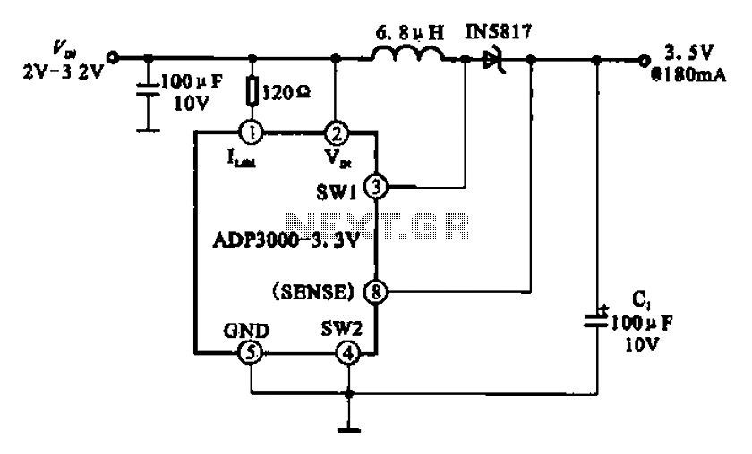
The boost regulator circuit is designed to increase a lower DC voltage, specifically from around 3V to a stable output of 3.5V. This circuit typically employs a switching regulator topology, which is efficient for converting voltage levels while minimizing power loss.
The primary component of this circuit is a boost converter IC, which integrates various functionalities such as a switching transistor, control logic, and feedback mechanisms. The input voltage is fed into the circuit, where it is stored in an inductor during the 'on' state of the switching cycle. When the switch turns 'off', the inductor releases its stored energy, which is then transferred to the output capacitor, raising the voltage to the desired level.
Key components of the circuit include:
1. **Inductor**: This stores energy when the switch is closed and releases it to the output when the switch is opened.
2. **Switching Element (Transistor)**: This is typically a MOSFET that alternates between on and off states to control the energy transfer.
3. **Diode**: A fast recovery diode is used to prevent backflow of current and to ensure that the energy from the inductor flows to the output capacitor.
4. **Output Capacitor**: This smooths out the voltage at the output, providing a stable DC voltage to the load.
5. **Feedback Resistors**: These are used to create a voltage divider that feeds back a portion of the output voltage to the regulator IC to maintain the desired output voltage level.
The circuit may also include additional components such as input and output capacitors for filtering, as well as protection features like overcurrent protection and thermal shutdown to ensure reliable operation. The design must consider the load requirements, switching frequency, and efficiency to optimize performance.
When implementing this circuit, attention should be paid to the layout to minimize electromagnetic interference and ensure stable operation across varying load conditions. Proper thermal management should also be considered, as boost converters can generate heat during operation. Boost 3.5V regulator circuit With this chip can boost or build stable voltage supply to V ~ 3.V DC voltage into a DC voltage of 3.5 V,
Related Circuits

Have you ever accidentally left your front door ajar and had a pet escape? This circuit offers a smart solution to this problem. It is relatively simple yet serves as an excellent example. The circuit designed to prevent pets from...
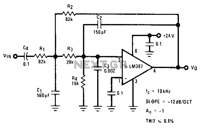
The circuit provides a passband gain of 1 with a corner frequency of 10 kHz, designed to eliminate high-frequency noise such as hiss, ticking, and popping sounds. This circuit operates as a low-pass filter, effectively attenuating frequencies above the specified...
The thermocouple cold junction compensation circuit and the MAX6675 converter circuit diagram form a temperature measuring system. The system utilizes a K-type thermocouple connected to the T terminals of the MAX6675, with the cold junction grounded. An 8051 microcontroller...
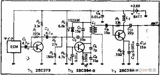
The circuit functions as a frequency modulation (FM) transmitter that operates within the 76 to 90 MHz FM radio band, commonly referred to as a wireless microphone. It receives signals through an FM radio receiver. The circuit is capable...
555 timer circuits LM555 - Astable Oscillator Calculator, Capacitor Calculator, Basic Circuits for the LM555 Timer, Triggering and Timing Helpers for Monostable Timers, Controlling Circuits for LM555 Timers, Advanced Circuits for the LM555 Timer, LM556 Timers with Complementary or...
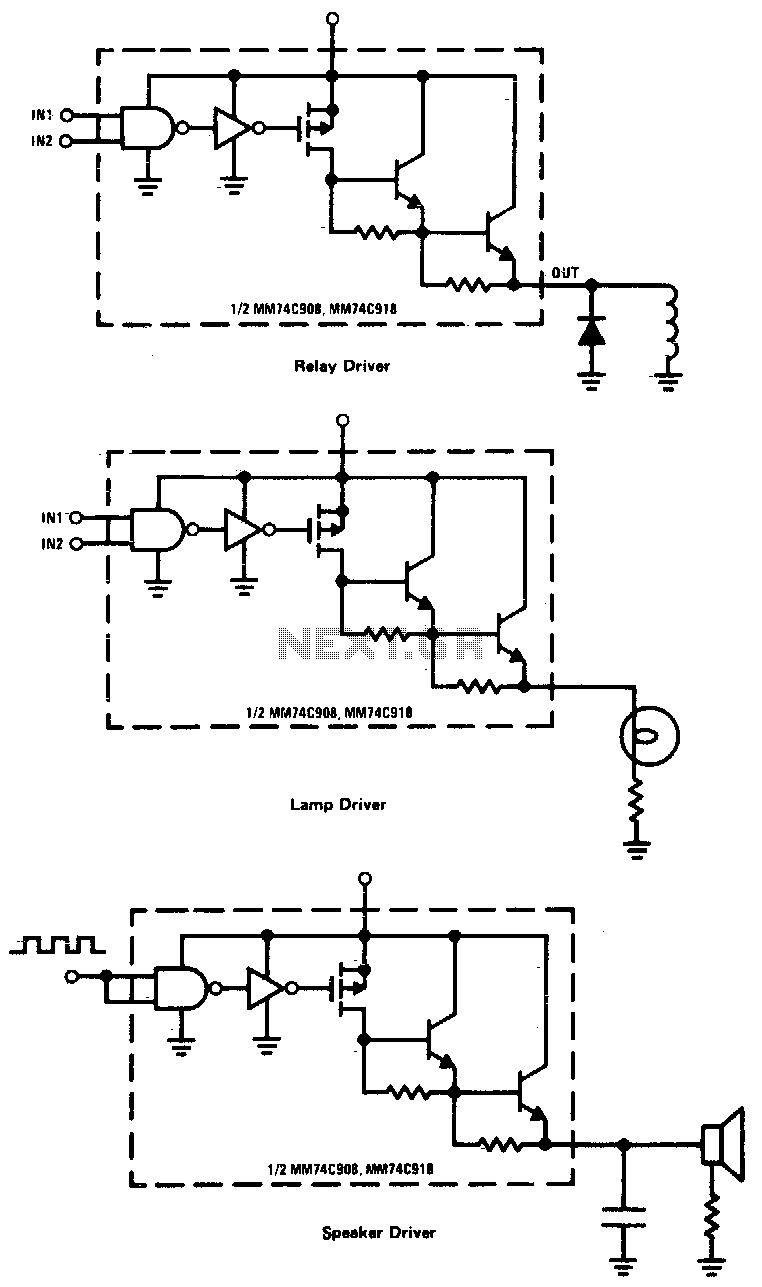
CMOS drivers for relays, lamps, speakers, and similar applications provide extremely low standby power consumption. When operating at Vcc = 15 V, the power dissipation per package is typically 750 nW when the outputs are not drawing current. Consequently,...