
Boss SD-1 Super OverDrive guitar pedal schematic diagram

The Boss SD-1 Super OverDrive pedal operates by processing the input guitar signal through a well-defined signal path that enhances tonal characteristics while introducing overdrive. The uPC4558C dual operational amplifier serves a crucial role in amplifying the guitar signal, where the first half of the op-amp is configured to provide initial gain and drive the subsequent clipping stage. The use of three silicon diodes in the feedback loop introduces a unique clipping behavior, characterized by asymmetry; this means that the harmonic content generated during overdrive is richer and more complex, contributing to the pedal's signature sound.
The tone control circuit, which is a significant differentiator from the OD-1, allows users to shape their sound further by adjusting the frequency response. The level control circuit provides the ability to set the output volume, ensuring that the processed signal can be matched to the desired level for amplification or recording.
The output buffer, implemented with Q6, ensures that the signal is adequately driven to the next stage, whether it be an amplifier or another effect pedal, maintaining signal integrity and minimizing loss. The bypass circuit, utilizing JFETs Q1 and Q2, allows for a true bypass functionality, ensuring that when the pedal is not in use, the guitar signal remains unaffected by the internal circuitry. Meanwhile, the bistable multivibrator formed by Q3 and Q4 provides a reliable switching mechanism, enhancing the pedal's overall performance and usability.
In summary, the Boss SD-1 Super OverDrive is a meticulously designed pedal that combines simplicity with effective circuitry to produce a rich, dynamic overdrive sound, making it a popular choice among guitarists seeking to emulate the warmth and character of tube amplification.The Boss SD-1 Super OverDrive is a pedal with a simple design, using only one dual operational amplifier (uPC4558C) and 6 transistors, with an asymmetric overdrive circuitry for a classic, natural tube amp growl. It generates the warm distortion of an overdriven tube amplifier while maintaining the subtle nuances of a guitar player`s picking techn
ique. The schematic is nearly identical to the classic OD-1 OverDrive, the only major difference is the tone control circuit. The design is simple and easy to follow: the guitar signal is buffered with Q5 and enters the first half of the uPC4558C dual operational amplifier.
There are 3 silicon diodes in the negative feedback path of the op-amp. Two diodes are in one direction and only one in the other. This arrangement produces asymmetrical soft clipping - one side of the waveform is clipped more severely than the other. The tone corrector and level control circuits are next. The signal finally exits the circuit after the output buffer made with Q6. The bypass circuit uses a classic arrangement with 2 JFETs (Q1 and Q2) serving as solid-state switches and a symmetrical bistable multivibrator made with Q3 and Q4.
🔗 External reference
Related Circuits
The purpose of this timer is to disconnect the compressor circuit and connect a resistive heating element located near the evaporator at regular time intervals. The defrost heater is controlled by a thermostat and is used to melt any...

The drop-down category menus above may help you find what you are looking for. Be sure to also look under the Bodo's Power by Topic sub-categories. They include topics similar to our general categories. If the above suggestions were...
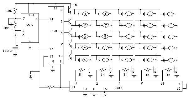
This circuit is same as the above setup to drive 25 small Xmas lights. The lights operate at about 200mA and 3 volts. The supply voltage is set to 5 volts and the 4017 counter output will drop about...
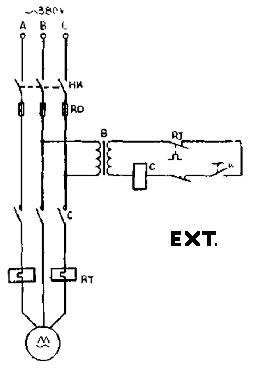
The gear lathe is unloaded from the stop line as depicted in the figure. When the turning clutch is in the stop position, the limit switch XWK is disengaged, which immediately powers the AC contactor coil C to stop...
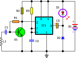
The circuit flashes an LED when detecting an incoming call and is powered by a single 1.5V cell. It is designed to detect incoming calls in a cellular phone. This circuit utilizes a simple yet effective approach to alert users...
The circuit diagram for an electric start and stop timer is illustrated in the following cycle. It utilizes the LM555 integrated circuit configured as an adjustable duty cycle multivibrator. The circuit includes components C3, KH1, W1, KH2, and W2,...