
Electrical circuit diagram cycled on and off timer
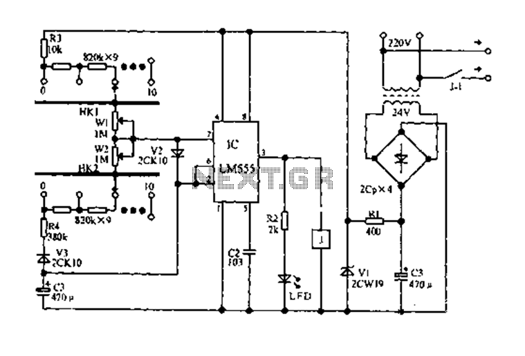
The electric start and stop timer circuit employs the LM555 timer IC, which is renowned for its versatility in timing applications. In this configuration, the LM555 operates in astable mode, allowing it to generate a continuous square wave output. The timing intervals are determined by the values of the resistors (R3, HK1, HK2) and the capacitor (C3), which define the charging and discharging times.
The circuit begins with the application of power, initiating the charging process of capacitor C3 through the resistive components. As C3 charges, the voltage across it increases until it reaches the threshold level of 2/3 of the supply voltage. At this point, the LM555's internal flip-flop changes state, resulting in a high output signal at pin 3. This output signal is used to drive an LED indicator and activate relay J, which connects the load to the power source.
Simultaneously, the circuit begins the discharge phase of capacitor C3. This is facilitated through the discharge path involving V3, R4, and the resistances of HK2 and W2. The discharge occurs until the voltage across C3 falls to 1/3 of the supply voltage, at which point the LM555 toggles again, deactivating relay J and disconnecting the load.
The design incorporates adjustable elements (W1, W2) that allow for fine-tuning of the timing intervals. Each of these potentiometers can modify the resistance in the charging and discharging paths, effectively altering the time constants of the circuit. This flexibility enables a delay adjustment range of 0-5 minutes, while the overall coarse and fine adjustments provided by HK1 and HK2 can extend the delay period by approximately 4.5 minutes.
In summary, this timer circuit is capable of providing precise control over timing applications, making it suitable for various electronic projects where timed activation and deactivation of loads are required. The simplicity of the LM555 timer, combined with adjustable components, allows for a user-friendly experience in achieving desired timing outcomes.Electric start and stop the timer circuit diagram shown in the following cycle, LM555 adjustable duty cycle when the base integrated circuits multivibrator, the C3 charge-disch arge circuit in series KH1, W1, KH2, W2, respectively, as electrical open, stop time coarse and fine adjustment. When the circuit operates power through R3, HK1 series resistance and W1, V2 charging to C3, 3 feet high output of IC, LED lights, the relay J pull its contacts connected load.
When C3 voltage rises to 2/3 supply voltage, IC flip, relay releases. Meanwhile, C3 through V3, R4, 7 feet on HK2 series resistance W2 and IC-to-ground discharge. When the voltage drops to 1/3 C3 supply voltage, IC flip relay. So the cycle work. HK1, HK2 each block can increase or decrease the delay of 4.5 minutes, W1, W2 of the adjustment range of about 0-5 minutes.
Related Circuits

This circuit is a robust and efficient power amplifier suitable for various audio applications. It delivers 60W RMS output at a 50V supply with an 8 Ohm load. The design is user-friendly, allowing for the use of non-critical components...
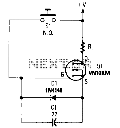
When switch S1 is pressed, capacitor C1 begins to charge to the supply voltage. This action creates a forward bias on the gate of transistor Q1, turning it on and allowing current to flow to the load resistor RL....
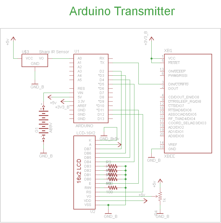
The schematic for the transmitter in this project consists of four main components: the Arduino UNO, the Sharp IR distance sensor, the XBee wireless modules, and a 16x2 LCD. The connections between these components are illustrated in the schematic....
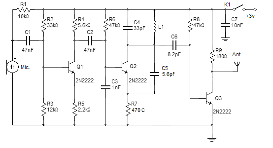
This FM wireless microphone is straightforward to construct and offers significant transmission capabilities, with a range of approximately 300 meters outdoors. Its compact component count and 3V operating voltage allow it to effectively penetrate multiple floors of an apartment...
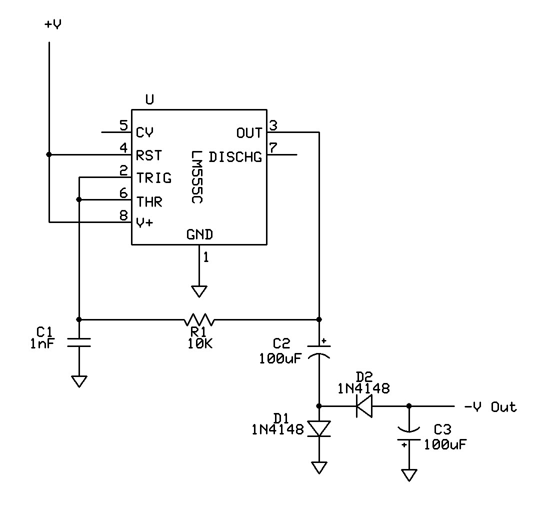
Can a 555 negative supply circuit, like the one below I pulled from another schematic, supply enough negative voltage to an LM324 and an AD736JN? The 555 timer integrated circuit can be configured to generate a negative voltage supply,...
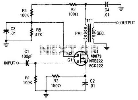
A MOSFET is utilized as a wideband buffer amplifier. T1 is wound on a toroid of approximately specified diameter, using material suitable for the frequency range, typically between 1 MHz and 20 MHz. The turns ratio should be approximately...