
Buck Converter Design
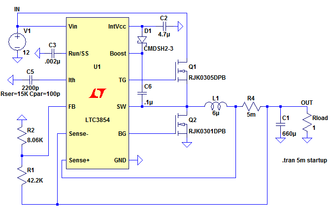
The described circuit operates as a buck converter utilizing the LTC3891 integrated circuit. The primary function of this converter is to step down the input voltage from 24V to a regulated output voltage of 5V while delivering a maximum load current of 2A. The operation begins with the top MOSFET (Q1) being activated, which initiates the current flow through the inductor (L1). The inductor current increases linearly due to the voltage across it, which is determined by the input voltage and the output voltage.
As the output voltage rises, the control mechanism within the LTC3891 monitors the current through a sensing resistor (R4). Once the sensed voltage across R4 reaches a predetermined threshold, the LTC3891 deactivates Q1, allowing the inductor to maintain its current flow. This is critical because inductors resist rapid changes in current. The bottom MOSFET (Q2) is then activated to clamp the inductor to ground, maintaining the current flow and preventing voltage spikes that could damage the circuit components.
The design also incorporates a flying capacitor (C6), which is charged during the operation to provide the necessary gate drive voltage for the top MOSFET. This capacitor is charged to a voltage higher than the input voltage, ensuring that Q1 can be turned on effectively after Q2. The feedback mechanism ensures that the output voltage remains stable, adjusting the duty cycle based on load conditions. The converter operates in continuous conduction mode (CCM) under normal conditions, maintaining efficiency and performance even with varying load currents.
The circuit's performance can be simulated using LTspice or similar software, allowing for analysis of current waveforms and verification of design parameters. The characteristics of the inductor, the switching frequency, and the load conditions are all crucial factors in determining the efficiency and stability of the buck converter. Overall, the LTC3891 provides a robust solution for voltage regulation in applications requiring step-down conversion from a higher input voltage while maintaining efficiency and output stability.The top MOSFET switches on creating a short circuit between the input voltage (IN) and the left hand side of the inductor, L1. The inductor current ramps up according to the equation where V is the voltage across the inductor, L is the inductance value and di/dt is the change in current with time through the inductor.
Thus with a fixed input volta ge and a fixed output voltage, there is a fixed voltage across the inductor thus the change in current with time is constant (i. e. a ramp waveform). The output voltage on startup is 0V, so the initial voltage across the inductor is equal to the input voltage.
However, as the output voltage changes (and then reaches regulation) the above equation becomes The peak inductor current is sensed by a small series resistor, R4, and when the voltage across this resistor equals a certain value (see the specific converter`s datasheet) the IC switches off the top MOSFET. Now, inductors do not like having their current interrupted, so when the top MOSFET switches off, the inductor behaves like a battery to try to maintain the current flow.
Referring to FIG 1, output side of the inductor tries to fly positive (to push current out of the right hand side of the inductor) and its switched side (the left hand side) flies negative (to try and sink current into its left hand side) in an effort to maintain the left to right current flow. Since the output side of the inductor is clamped by a capacitor, the left hand side flies negative. At this point the IC switches on the bottom MOSFET, Q2, to clamp the left hand side of the inductor to ground and enable the inductor to maintain its current flow.
When MOSFET Q2 switches on, it also provides a short circuit to 0V at the bottom of capacitor C6. Since the top of C6 is connected to the LTC3891`s internal linear regulator (INTVCC) via diode D1, this capacitor charges to INTVCC 0. 3V. The voltage on this capacitor is then used to provide a voltage higher than the input voltage to enable the top MOSFET to be switched on.
Indeed, at startup, Q2 actually switches on before Q1 to charge the flying capacitor, C6, to enable Q1 to be switched on. FIG 2 shows an LTspice simulation with the current ramping from 4. 378A to 5. 604A over 1. 08us, a change of 1, 135, 185 Amps per second not too far off what was calculated above. It is interesting to note that the value of di/dt is determined ONLY by the inductance value and the voltage across the inductor.
The controller IC has nothing to do with setting the inductor ramp current. It is also useful to calculate the duty cycle of the converter. The duty cycle is the ratio of the ON time of the top MOSFET to the total period of oscillation. It is interesting to note that the duty cycle is purely dependent on the input and output voltages and has nothing to do with the controller IC or inductor value. The above is true as long as the inductor current does not fall to zero. The converter is then said to be operating in continuous conduction mode (CCM). If the inductor current ramps down to zero, the converter is then in discontinuous conduction mode (DCM).
In CCM if the load current changes, the duty cycle of the converter and the amplitude of the ripple current remain the same. The circuit responds to a change in load current by changing the midpoint of the inductor current (its dc offset).
Indeed it is also true that the average inductor current in a buck converter is equal to the load current. In FIG 2 we can see that the midpoint of the inductor current is 5A and it can be seen from FIG 1 that our load is 1 Ohm, thus the load current is 5A.
If the load resistance were increased to 2 Ohms, the ripple current and duty cycle would remain unchanged (in the steady state), but the dc offset current would fall to 2. 5A. We are going to use the LTC3891 to design a buck converter that converts from 24V to 5V and can supply a load of 2A.
The LTC3891 datasheet can be dow 🔗 External reference
Related Circuits
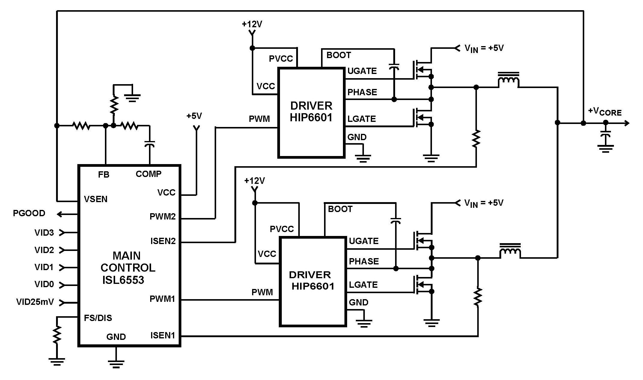
The ISL6553 multiphase PWM control IC, along with its associated gate drivers (HIP6601, HIP6602, or HIP6603), establishes a precise voltage regulation system tailored for advanced microprocessors. Multiphase power conversion represents a significant evolution from traditional single-phase converter configurations, addressing...
In electronics, a digital-to-analog converter (DAC or D-to-A) is a device that converts a digital code, typically in binary format, into an analog signal, which can be in the form of current, voltage, or electric charge. DACs are utilized...
This varactorless high-frequency modulator electronic project must be powered by a simple DC 3-volt power source, such as a 3-volt battery. Traditionally, high-frequency oscillators are frequency-modulated using a varactor. However, varactors typically require a significant voltage change to achieve...
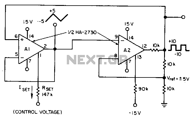
This circuit utilizes a programmable operational amplifier, specifically the HA2730, which is a two-amplifier monolithic chip featuring independent programming ports for each amplifier. The parameters of the amplifiers, including the slew rate, vary linearly based on a set current....
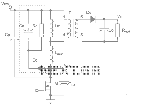
The work process analysis circuit diagram illustrates the use of a flyback converter transformer model. The flyback transformer primarily consists of ideal transformer magnetizing inductance and leakage inductance components. The flyback converter circuit exhibits high-frequency resonance at both ends...
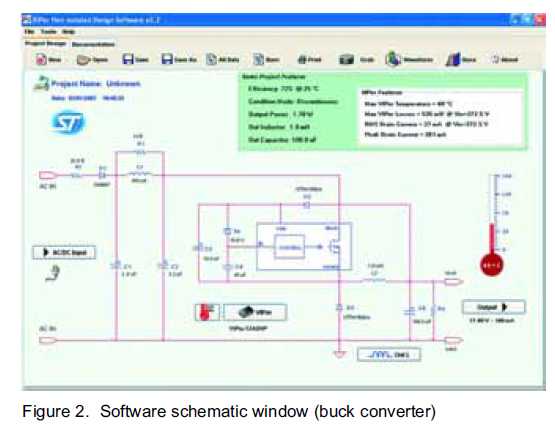
The new VIPer12A and VIPer22A software can be utilized to supply the numerous electronic components needed for home appliances. Various power supply topologies may be employed. The VIPer12A and VIPer22A are integrated circuits designed for power supply applications, particularly suitable...
Warning: include(partials/cookie-banner.php): Failed to open stream: Permission denied in /var/www/html/nextgr/view-circuit.php on line 713
Warning: include(): Failed opening 'partials/cookie-banner.php' for inclusion (include_path='.:/usr/share/php') in /var/www/html/nextgr/view-circuit.php on line 713