
Buffer Lc Data And Clock Lines Circuit
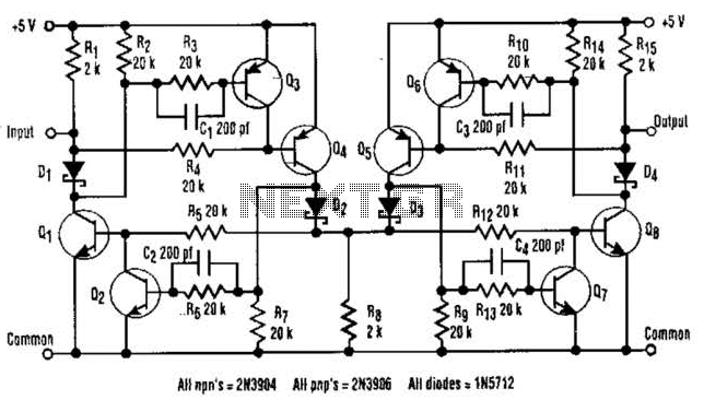
The capacitors in the circuit mitigate switching glitches by ensuring that the inhibit transistors deactivate before the output transistors. The operation of the circuit can be demonstrated through an example: when the input is high, Q4 turns off, and the voltage across R8 drops to zero. This results in Q1 and Q8 turning off, causing the output to return to its normal high state. When the input is pulled low, Q4 is activated. Diode D1 remains reverse-biased, preventing Q3 from deactivating Q4. With Q4 active, current flows to both Q2 and Q1, turning them on; however, Q2 activates first to keep Q1 off, preventing latching. Q4 also activates Q8. Diode D4 becomes forward-biased, turning on Q6, which then deactivates Q5. With Q5 off, Q7 remains inactive, and the output stays low. The circuit will not latch even when both the input and output are externally driven low. Using the component values shown in Figure 2, the circuit achieved a clock rate of 80 kHz with a VOH of 5.0 V and a VOL of 0.5 V.
The I2C bus architecture is designed to facilitate communication between multiple devices with minimal wiring, utilizing only two lines: the Serial Data Line (SDA) and the Serial Clock Line (SCL). Each device on the bus can act as either a master or a slave, allowing for flexible communication protocols. The open collector outputs enable multiple devices to connect to the same bus without interference, as devices can only pull the line low, leaving it high when inactive, thanks to the pull-up resistor.
In the described non-latching buffer circuit, the use of transistors (Q1, Q2, Q3, Q4, Q6, Q7, and Q8) is crucial for maintaining the integrity of the signal while preventing unintended latch-up conditions. The design also incorporates capacitors to filter out any noise or glitches that might arise during switching, ensuring stable operation at higher frequencies. The careful arrangement of the components, particularly the forward and reverse biasing of the diodes, is essential for controlling the flow of current and ensuring that the circuit remains in the desired state without latching.
The performance metrics achieved by the circuit, such as the 80 kHz clock rate, demonstrate its capability for high-speed applications, making it suitable for various real-time communication scenarios in embedded systems and other electronic applications. The voltage levels of VOH and VOL indicate the circuit's compatibility with standard logic levels, ensuring seamless integration with other digital components. Overall, this non-latching buffer circuit enhances the functionality of the I2C bus by providing a reliable means to expand the network while maintaining signal integrity. The I2C serial bus is a popular two-wire bus lor small-area networks. I2C Clock and Data lines have open collector (or drain) outputs for each device-on the network. Only a single pull-up resistor is needed. With this arcliitecture, each device can talk on the network, rather than just listen. In some circumstances, it might be desirable to buffer these lines to expand the network, which can sometimes be a tricky task. The obvious approach (Fig. 1) wont work because it latches in either the higher or lower state. A circuit for a noninventory nonlatching buffer is also shown.The circuit is symmetrical about its center so that the input and output can be swapped.
Ql and Q8 are the output open collector drivers. Q2, Q3, Q6, and Q7 provide the nonlatching functions. The capacitors prevent switching glitches by ensuring the inhibit transistors turn off before the output transistors do.Operation can be best explained by example: if the input is high, Q4 turns off, and the voltage across R8 goes to zero. This turns off Ql arid Q8. The output then goes liigh, which is the circuit`s normal resting place. If the input is pulled low, Q4 is turned on.Diode D1 remains reverse-biased, preventing Q3 from turning off Q4.
With Q4 on, current is supplied to both Q2 and Ql to turn them on, but Q2 turns on first to keep Ql off. This prevents the input from latching. Q4 also turns on Q8. D4 is now forward-biased, so Q6 turns on, and thus turns off Q5. With Q5 off, Q7 will not turn on. The output remains low. Even with both the input and the output externally driven low, the circuit will not latch. The circuit, using the values shown in Fig. 2, reached a clock rate of 80 kHz with a VOH of 5.0 V and a VOL of 0.5 V. 🔗 External reference
Related Circuits

The system includes a CD player, amplifier, speakers, power supply, and headphones. The Mitsumi CD player, designed for the United States, features a 4-speed CD-ROM launched in mainland China in 1997, equipped with an out-of-box key panel for speed...
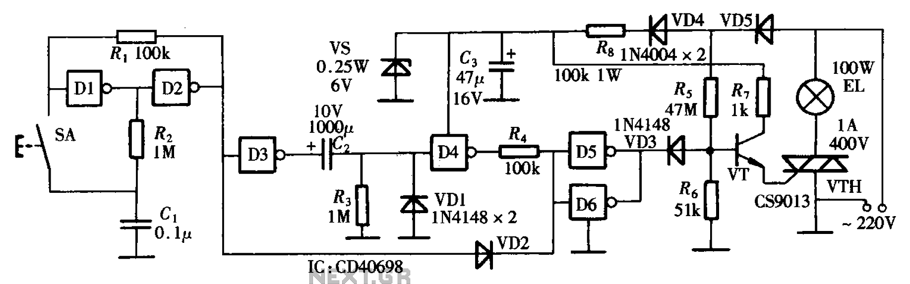
The bedside door fixture delay circuit features a straightforward design and offers cost-effectiveness. It is constructed using a hex inverter CD4069. The bedside door fixture delay circuit employs the hex inverter CD4069, which is a versatile integrated circuit (IC) commonly...
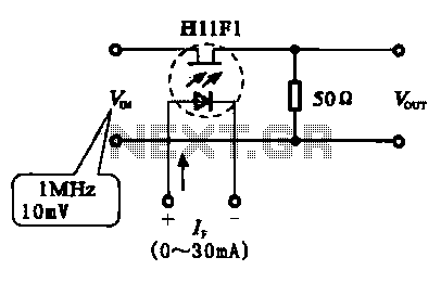
A phototransistor, also referred to as a photosensitive transistor, is primarily utilized as a photosensitive device. It is characterized by its ability to adjust impedance in relation to the intensity of incoming light, similar to that of photosensitive resistors...
This circuit will drive a small DC motor over a wide range of speeds without stalling by controlling the duty cycle of the motor, rather than the supply voltage. The described circuit utilizes pulse width modulation (PWM) to effectively control...
The kit employs an off-the-shelf microcontroller based on the AtMega328P-PU Arduino, along with a simplified version designed for ease of replication and modification by collaborators and students. This initiative aims to enable the fabrication of simplified microcontrollers for DIY...
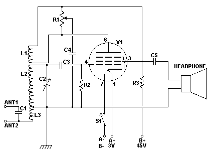
A regenerative radio operates by feeding back a small portion of the amplified output from the detector into the input. This feedback mechanism enhances sensitivity significantly beyond what a detector can achieve on its own. The simple regenerative radio...
Warning: include(partials/cookie-banner.php): Failed to open stream: Permission denied in /var/www/html/nextgr/view-circuit.php on line 713
Warning: include(): Failed opening 'partials/cookie-banner.php' for inclusion (include_path='.:/usr/share/php') in /var/www/html/nextgr/view-circuit.php on line 713