
Carrier-Current Receiver For Data Transmission

The described receiver circuit is a sophisticated assembly designed for processing frequency-shift keying (FSK) signals within a specified operational bandwidth of approximately 100 kHz. The circuit architecture includes several key components that work in unison to ensure effective signal detection and amplification.
At the heart of the receiver is the input network, which is responsible for conditioning the incoming signal before it is amplified. The amplifier IC7 is a critical component that boosts the strength of the received signal, ensuring that it is adequately processed by subsequent stages. Following amplification, the signal is routed to the FSK Phase-Locked Loop (PLL) detector IC8, which demodulates the frequency-shifted signal back into its original data format.
The output stage of the receiver comprises a series of amplifiers and interfaces, specifically Q2, Q3, IC3A, and IC3B. Among these, the 1488 Quad RS232 line driver is utilized to convert the processed signal into a format suitable for transmission over RS232 communication lines. This conversion is essential for compatibility with standard serial communication protocols, allowing for seamless integration with other devices.
The circuit's design includes specific component values that are optimized for operation in the intended frequency range, ensuring reliable performance. The recovered data is available at pins 5, 6, and 7 of the PLL detector, which serves as the output to the amplifier/interface circuit. This output stage is crucial for driving any subsequent processing or display components, facilitating the effective use of the received data.
Furthermore, this receiver circuit is designed to operate in conjunction with a carrier-current data transmitter, forming a complete communication pair. This synergy between the transmitter and receiver allows for efficient data transmission and reception, making it suitable for various applications in electronic communication systems. Overall, the design reflects a careful balance of amplification, signal processing, and output interfacing, tailored for high-performance operation in the specified frequency range. This receiver consists of an input network amplifier IC7 FSK PLL detector ICG, and output am plifier/ interface Q2, Q3, IC3A and IC3B, a 1488 Quad RS232 line driver of the carrier-current signal. Tuned amplifier IC7 amplifies this signal and drives PLL detector IC8. The values shown in the circuit are suitable for operation in the 100-kHz range. Recovered data at pins 5, 6, 7 is fed to the output amplifier/interface circuit (Fig. 6). This circuit is also used with the carrier-current data transmitter to form a pair.
Related Circuits
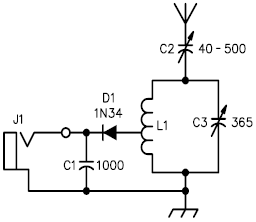
A crystal radio receiver is a very simple radio receiver that requires no battery or external power source, operating solely on the energy harvested from radio waves through a long antenna. A crystal radio receiver is a passive radio receiver...
The board features a small power supply that generates 3.3V at 250mA. The built-in 3.3V regulator on the Arduino is not utilized because it is only guaranteed to provide up to 50mA, which may not be sufficient for some...
The CD-ROM 48X RF AMP Chip serves as an RF pre-signal processor, handling signals from the optical pick-up. This chip processes the primary signal through a summing amplifier, an automatic gain control (AGC) block, and an equalization (EQ) block,...
This project originated from an interest in a new form of radio transmission known as Digital Radio Mondial (DRM). The Digital Radio Mondial (DRM) is a revolutionary digital broadcasting technology designed for AM and FM radio. It provides enhanced audio...
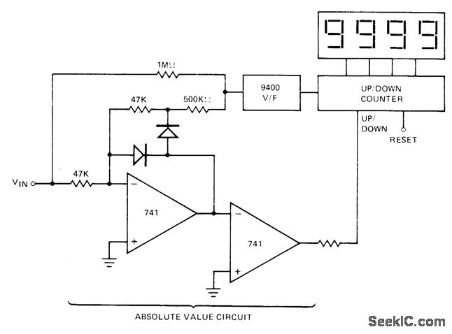
The absolute-value integrator circuit generates the effect of producing negative frequencies when the input signal is negative. It accomplishes this by allowing the counter to count up for positive voltage and count down for negative voltage. The specific types...
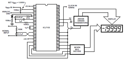
The schematic below shows the ICL7135 integrating analog-to-digital converter (ADC) functional diagram. According to the datasheet, an integrating converter is the right choice for panel meters and digital voltmeter applications. It can also be used for reducing line frequency...