
CCD analog output signal processing circuit diagrams
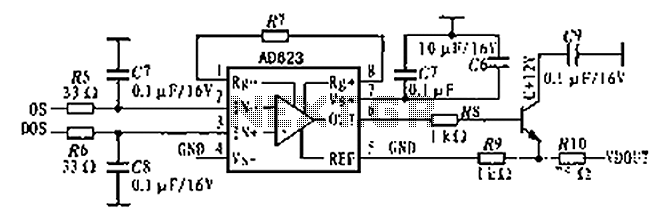
The AD623 amplifier is designed for applications requiring precise signal amplification with minimal interference from common-mode signals. Its high CMRR ensures that differential signals can be accurately amplified while rejecting noise and interference that may be present in the common mode. The low voltage drift characteristic is critical for applications where stable performance over varying temperatures is essential.
The programmable gain control feature allows users to set the gain of the amplifier according to the specific requirements of the application, which can be achieved by connecting an external resistor to the appropriate pins. This flexibility makes the AD623 suitable for a wide range of applications, particularly in sensor signal processing where the input signal levels may vary significantly.
In the context of CCD analog signal processing, the AD623 plays a crucial role in maintaining signal integrity. The amplifier's design facilitates the handling of video signals, which are often subject to fluctuations and noise. By compensating for the inverting and non-inverting inputs, the amplifier ensures that the output signal remains stable and reliable.
The output stage of the AD623 is configured as an emitter follower, which enhances the amplifier's ability to drive loads effectively. This configuration provides a high input impedance and low output impedance, allowing for efficient signal transfer to subsequent stages in the circuit without significant signal degradation.
Overall, the AD623 is an effective solution for applications demanding high precision and stability in signal amplification, particularly in environments where temperature variations and common-mode noise are concerns. Its integrated design simplifies circuit implementation while improving overall performance.AD623 integrated 3-way amplifier. Single or dual supply can work with high CMRR and low voltage drift, programmable gain control in addition to an external resistor, all compon ents are integrated in the interior temperature of the circuit to improve the stability and reliability. Application of AD623 in CCD analog signal processing circuit shown. The video signal output, respectively, and compensation to the AD623 inverting and non-inverting input.
In AD623 output stage emitter follower termination to enhance the driving capability of the signal. The selection device can eliminate the use of ordinary temperature op amp and peripheral resistance caused by the output signal drift.
Related Circuits
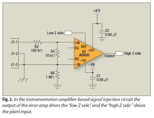
A signal-injection circuit for control-loop analysis is flat from DC to 200 kHz, isolated from chassis ground, and easily constructed with a readily available instrumentation amplifier. The signal-injection circuit is designed to facilitate control-loop analysis by providing a stable and...
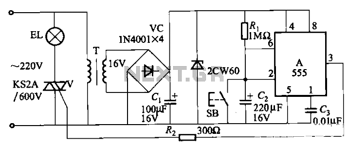
The circuit utilizes a 555 timer IC to create a lighting group delay effect, as illustrated in Figure 2-46. It consists of the 555 IC along with a resistor and capacitor configuration that establishes the delay. The circuit remains...
Is the battery empty, or is there something wrong with the device? This question often arises when troubleshooting a battery-powered device, such as a Walkman. When diagnosing issues with battery-powered devices, it is essential to systematically evaluate both the battery...
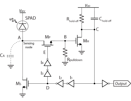
VLQC is a quenching circuit developed in the laboratory to meet the specific requirements of an array, including high compactness, cross-talk avoidance, and low afterpulsing. In the VLQC design, a single transistor is utilized to perform the sensing, quenching,...
Here is a design circuit for a frequency modulator that is equipped with a tuning circuit. In this circuit, a pair of 1N4007 diodes is utilized as varactor diodes. The choice of 1N4007 diodes is not due to their...
Individuals seeking a distinctive gift for Christmas and New Year may find this project appealing. Certification of this project will undoubtedly create a preference for it. The project in question appears to be a creative endeavor aimed at providing a...
Warning: include(partials/cookie-banner.php): Failed to open stream: Permission denied in /var/www/html/nextgr/view-circuit.php on line 713
Warning: include(): Failed opening 'partials/cookie-banner.php' for inclusion (include_path='.:/usr/share/php') in /var/www/html/nextgr/view-circuit.php on line 713