
CD4011 dual-produced sound and light control delay lamp circuit
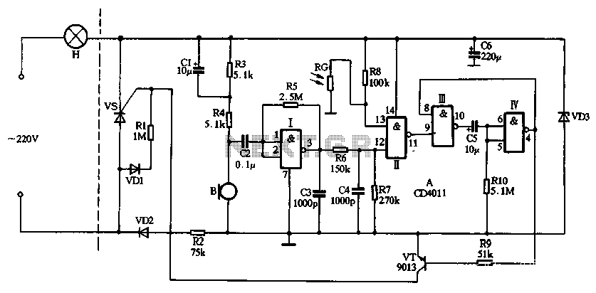
The circuit is designed to automatically control lighting based on ambient light levels and sound detection. The use of NAND gates allows for flexible logic configurations, making the circuit adaptable for various applications. The integration of a photoresistor ensures that the light remains off during the day while still being responsive to sound signals. This dual control mechanism provides an efficient solution for automated lighting systems, particularly in scenarios where hands-free operation is desired, such as in hallways or outdoor areas. The delay feature, implemented through the monostable configuration, ensures that the light remains on for a predetermined duration after sound activation, enhancing usability and energy efficiency. The inclusion of a half-wave rectifier circuit ensures that the integrated circuit receives a stable DC voltage, allowing for reliable operation of the entire system. Overall, this circuit exemplifies a practical application of digital logic in creating an intelligent lighting system that responds to environmental stimuli.Sound with CD4011 digital circuits made light lamp dual-control delay section circuit shown in Figure 3-17, the left portion of the dashed line in Fig general lighting lines, the right part is the sound and light control delay switch double circuit, SCR vs constitute lighting the main circuit switch, the control loop is two-input NAND gate CD4011 constitute four. NAND gate I composed a linear amplifier for amplifying the audio signal B microphone input. NAND gate II composed of light control switch, the NAND gate III, t composition monostable circuit. And NAND gate logic functions are: "See 0 1, all the l O". Daytime indoors light line is strong, light-sensitive resistors RO irradiated by light exhibits low resistance, so that the NAND gate II - inputs 13 feet low level "0", the output terminal II pin is high "l", it is 9 feet also as "l".
t two NAND gate inputs 5,6 feet because Rl0 ground to the low level "0", the nozzle output pin 4 is "1", 8 feet to "1." NAND gate III both inputs are "l", the output terminal IO pin to "0", low capacitance c5 both ends can not be charged, and the transistor VT due to the high base resistor R9 connected electrically and a half feet 4 Therefore VT conduction, vs VT gate is grounded off, lights are not bright. Since 13 feet low "o", so regardless of their 12 foot level changes, electronic switches are sealed bad E, the lamp can not be lighted.
In the evening, photoresistor RG light irradiation exhibit a high resistance, the resistance is much greater than R8, so] 3 feet high "l", which provided the conditions for the lights, but the output of 1 l foot level 12 foot level depends on the level of the case. When someone walking, pick up sound signal by B cz coupling into the NAND I zoom in, and then by R6 to C4 (charging time constant minimum) + 12 feet so that becomes a high level "l", in accordance with NAND gate "out of whole l 0" logic.
II pin output low level "0", 9 feet for the "O". From "See the 1 O" shows that IO pin is "l" that is 10 feet high output, the Rl0 to c5 charge. Root According to the principle of voltage across the capacitor is not mutated, 5,6 feet for the "l", so the output terminal 4 feet low "O", VT deadline, SCR vs the door to get forward by VD1 and Rl Ji opened contact current, lamp H powered light.
After about 30 seconds, c5 is fully charged, 5,6 feet returns low "O", 4 feet high output "l", VT hunt through, vs lose touch sent electric current when the AC zero crossing that off off, lights off. At steady state, 10 feet low "0", c5 by Rl0 discharge, ready for the next turn on the lights for the delay.
VD2, VD3, R2 and C6 form resistance voltage half-wave rectified line voltage, the output is about 6V DC, for the integrated circuit electricity.
Related Circuits
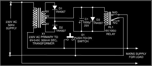
This is a low-cost protection circuit designed to safeguard electrically operated home appliances, such as TVs, DVD players, refrigerators, and other devices, during sudden power outages and the subsequent restoration of mains supply. Appliances like refrigerators and air conditioners...
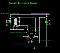
This is a simple intercom circuit utilizing the common IC LM380. In this configuration, the switch is set to the talk position for the speaker on the left, while the other participant is in the listening position. If the...
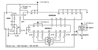
When the switch is opened, the timer generates an approximate 1-second clock signal, decrementing the counter until it reaches a count of zero. Upon reaching zero, the carry-out signal at pin 7 of the counter goes low, energizing a...
The shaft can be positioned at specific angular positions by sending a coded signal to the servo. As long as the coded signal is present on the input line, the servo will maintain the angular position of the shaft....
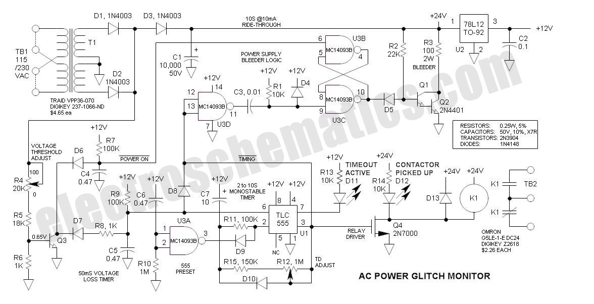
This AC Power Monitor continuously monitors the AC power line voltage for under-voltage conditions and missing cycles. When it detects a total of 5 or 6 consecutive anomalies, it triggers an alert. The AC Power Monitor is designed to provide...
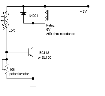
The following circuit illustrates a Light Barrier Sensor Detector Circuit Diagram. Features include a single transistor, an adjustable potentiometer, and a 6V power supply. The Light Barrier Sensor Detector Circuit is designed to detect the presence of an object by...
Warning: include(partials/cookie-banner.php): Failed to open stream: Permission denied in /var/www/html/nextgr/view-circuit.php on line 713
Warning: include(): Failed opening 'partials/cookie-banner.php' for inclusion (include_path='.:/usr/share/php') in /var/www/html/nextgr/view-circuit.php on line 713