
Cellphone Charger Using Bike Battery
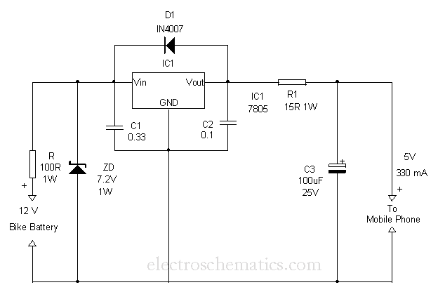
The circuit is built around a 12-volt motorcycle battery, which serves as the power source. The Positive Voltage Regulator IC 7805 is the core component that regulates the voltage to a stable 5 volts, suitable for charging mobile devices. The input to the regulator is protected by the Zener diode, which clamps the voltage to 7.2 volts, ensuring that the regulator operates within safe limits. The inclusion of diode D1 is crucial as it prevents damage from reverse polarity and protects against voltage surges that could occur during operation.
Capacitors C1 and C2, typically rated at 10µF to 100µF, should be placed as close as possible to the IC to reduce inductive effects and maintain stability during load changes. These capacitors help filter out noise and provide a smoother voltage output. Capacitor C3, often a larger value (e.g., 100µF to 470µF), serves as a reservoir to maintain a steady voltage during transient conditions, ensuring that the mobile device receives a consistent charging voltage.
In summary, this circuit design not only provides a reliable solution for charging mobile phones using a motorcycle battery but also incorporates essential protective features to safeguard the components from potential damage, ensuring longevity and reliability in various operating conditions.This is the simple and easy way to tap current from a Motor Bike battery to charge the Mobile Phone. Most of the Mobile Phone battery pack has three 1. 2 volt cells making the voltage to 3. 6 volts. For fast charging of the battery pack, each cell requires more than 1. 2 volts and sufficient current. This circuit can deliver 5 volts at 300 mA to char ge the battery quickly. The circuit is Voltage and Current regulated and with Polarity and Surge protection components. The circuit uses a Positive Voltage regulator IC 7805 to give 5 volt regulated output. The components around IC1 are meant for protecting the IC so as to give smooth output power. Zener diode ZD act as the Input Surge protecting diode. It provides 7. 2 volts to the input of the regulator IC from the 12 volt bike battery. Diode D1 is the Output Surge and Input Short protecting diode. When a surge voltage exceeding maximum voltage rating of the regulator is applied to the input or when a voltage in excess of the input voltage is applied to the output, the regulator will be destroyed. If the input terminal shorts with the ground, the output voltage increases above the input voltage(ground potential)and the charge in the capacitor connected to the output flows into the input side which is also fatal to the regulator.
Both these situations can be avoided by using the Zener at the input and the diode D1 across the regulator. Capacitor C1 and C2 provide stability to the regulator and these should be soldered close to the legs of the regulator.
Capacitor C3 act as a buffer to give constant voltage in the output. 🔗 External reference
Related Circuits

This circuit utilizes a 14-segment display to represent characters. The 14-segment display consists of 22 pins, which facilitate the display of various characters. Eight pins labeled A, B, C, D, E, F, K, and M are connected to the...

The circuit diagram represents an ultra-sensitive intruder alarm. A shadow from an intruder passing nearby is sufficient to trigger the alarm. The operational amplifier IC2 (uA 741) is configured as a sensitive comparator, with its set point determined by...
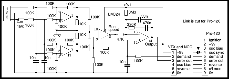
Most battery motor speed controllers are under manual control and the operator automatically adjusts speed to match demand. Under these conditions closed loop motor speed control is an unnecessary expense. However, when it is required, a tachogenerator can easily...
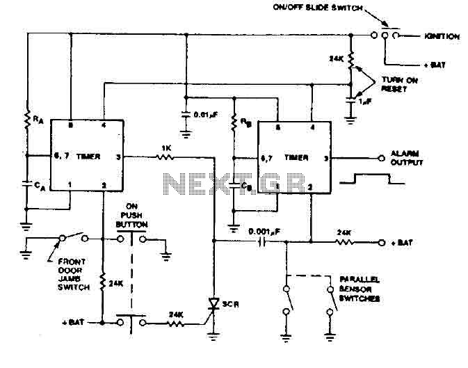
The 555 timer generates a reliable delay, enabling the driver to deactivate the alarm and eliminating the need for an external control switch that could be compromised. Additionally, the RCS prevents the activation of timer B unless it is...
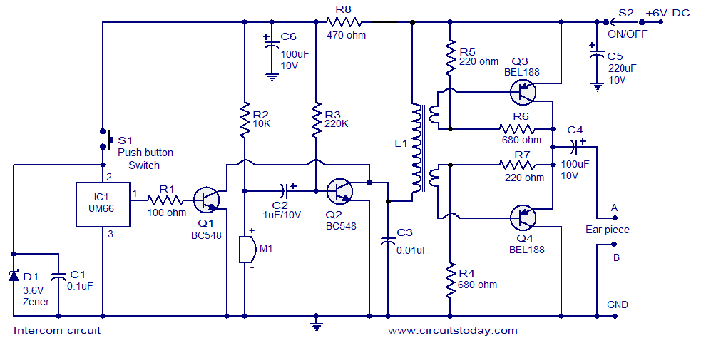
A straightforward intercom circuit designed using transistors. It does not require a changeover switch and can be used similarly to a telephone. This intercom circuit utilizes transistors to facilitate communication between two or more stations without the need for complex...
If a page name is not selected by pressing the button, the previously selected page name continues to be used. The value is stored in EEPROM and may be changed at any time. When the unit is first powered...
Warning: include(partials/cookie-banner.php): Failed to open stream: Permission denied in /var/www/html/nextgr/view-circuit.php on line 713
Warning: include(): Failed opening 'partials/cookie-banner.php' for inclusion (include_path='.:/usr/share/php') in /var/www/html/nextgr/view-circuit.php on line 713