
Cheap And Cheerful Transistor Tester
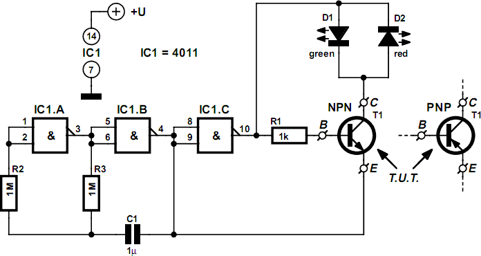
The transistor tester circuit operates by utilizing a quad NAND gate IC (CD4011B) to create an oscillator that drives the testing process. The oscillator is formed by connecting two of the NAND gates (IC1.A and IC1.B) with resistors R2 and R3 and capacitor C1, generating a square wave signal at pin 4. This square wave signal alternates between high and low states, which is crucial for testing the transistors.
When an NPN transistor is inserted into the circuit, the arrangement allows current to flow through LED D1 when pin 10 is high and pin 4 is low, indicating that the transistor is functioning correctly. The reverse bias condition occurs when the states of pins 10 and 4 switch, preventing current flow and allowing the LED to flash in sync with the oscillator's frequency. The same principle applies to the PNP transistor, where the conditions for forward bias are reversed, resulting in the red LED flashing.
The circuit's design ensures that the LEDs are driven within safe current limits, thus protecting the transistors being tested. The recommended supply voltage is critical for the operation, as exceeding 4.5 V could damage the transistor. The use of high-efficiency LEDs is recommended to ensure bright illumination while minimizing power consumption. Overall, this simple yet effective transistor tester provides a reliable method for quickly assessing the functionality of both NPN and PNP transistors in a compact design.By using a simple visual indicating system, this small transistor tester allows you to run a quick go/non-go` check on NPN as well as PNP transistors. If the device under test is a working NPN then the green LED (D1) will‚ash, while the red counterpart will‚ash for a functional PNP device.
However if the transistor is shorted, both LEDs will ‚ash, and an open-circuit device will cause the LEDs to remain off. The circuit is based on just one CD4011B quad NAND gate IC, four passive parts and two LEDs. The fourth gate in the IC is not used and its inputs should be grounded. Alternatively, you may want to connect its inputs and output in parallel with IC1. C to increase its drive power to the transistor test circuit. IC1. A and IC1. B together with R2, R3 and C1 form an oscillator circuit that generates a low-frequency square wave at pin 4. This signal is applied to the emitter of the transistor under test as well as to inverter IC1. C. The inverted signal from IC1. C and the oscillator output then drive the test circuit (LEDs, device under test, R1) in such a away that the voltage across that part of the circuit is effectively reversed all the time.
For example, with an NPN transistor under test, when pin 10 is High and pin 4, Low, current‚ows through LED D1 and the forward biased transistor. However, no current will‚ow when pins 10 and 4 change states, since the transistor is then reverse-biased.
The green LED, D1, will therefore‚ash at the rate determined by the oscillator. As you would expect to happen, a PNP transistor will be forward biased when pin 10 is Low and 4, High, enabling current to‚ow through the red LED in that case. A supply rail of around 3 V (two series connected 1. 5-V batteries) should be adequate. To prevent damage to the transistor under test, supply voltages higher than 4. 5 V should not be used. Because the LED currents are effectively limited to a few mA by the output of IC1. C (also slightly dependent on the supply voltage), it is recommended to use high-efficiency devices for D1 and D2.
🔗 External reference
Related Circuits
This continuity tester circuit allows for the examination of PCB track failures without the need to visually inspect the routing of the tracks, which can often be frustrating. The continuity tester circuit is designed to facilitate the detection of faults...
This circuit features a very stable and simple FM transmitter design. This transmitter can achieve a range of approximately 200 meters when properly matched. The FM transmitter circuit typically consists of several key components: an oscillator, modulator, amplifier, and antenna....

Logic-1 and logic-0 represent the states of digital signals, where logic-1 corresponds to a high voltage close to Vcc, and logic-0 corresponds to a voltage near neutral or ground. Logic-0 cannot be transformed into logic-1, while logic-1 can revert...

Here is a very simple yet practical circuit designed to check the type of LAN cables (straight or cross) as well as to identify possible faults. The circuit utilizes a unit with 8 outputs, each producing a pulse successively,...
The key to avoiding instability (motor-boating) in a high-gain circuit is to power the speaker using a separate power supply. This circuit design allows for the connection of one or two additional stations. It is recommended to construct the...
This circuit is designed for low power operation and can be tuned to function within the frequency range of 87-108 MHz, achieving a transmission distance of 20 to 30 meters. The circuit utilizes a pair of BC548 transistors, which,...