
In System Programming (ISP) for ATMEL chips
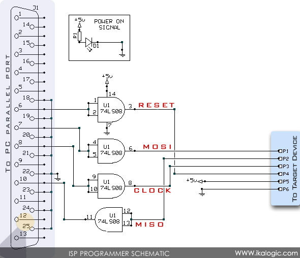
The ISP process is a critical aspect of microcontroller programming, enabling efficient and flexible updates without requiring physical access to the chip. The four lines used in ISP—MOSI, MISO, SCK, and RST—form a compact interface that simplifies connections while maintaining functionality. The choice of components, such as the 74HC08 or 74HCT08, enhances the robustness of the circuit, allowing for longer transmission lines without signal degradation. The use of buffers in the design protects the parallel port from potential damage, ensuring reliable operation during programming sessions.
The PCB layout must be meticulously designed to accommodate the parallel port connections and ensure that the necessary ground connections are properly established. The inclusion of a jumper wire for grounding simplifies the assembly process while maintaining the integrity of the circuit. Additionally, the placement of the crystal oscillator or external clock source is crucial for achieving the desired timing characteristics, which directly influence the programming speed and reliability.
In conclusion, the ISP method provides a practical approach to microcontroller programming, combining simplicity and effectiveness. The detailed understanding of the circuit operation, along with careful attention to component selection and PCB design, is essential for successfully implementing an ISP solution in microcontroller projects.ISP is a way to serially program your microcontroller, while it resides in its place, in other words, without removing the chip from your board. Whether you`re just starting in the ATMEL microcontrollers, or you`re familiar with it, ISP (In System Programming) will provide you a simple and affordable home made solution to program and debug your microcontroller based project.
Sometimes, ISP can become very useful, when adjusting some delays, frequencies or any other values that you would intend to find by trial and error. a process that would otherwise take too much time. Normally, the flash memory of an ATMEL microcontroller is programmed using a parallel interface, which consists of sending the data byte by byte (using eight independent lines for the data, and another bunch of lines for the address, the control word and clock input).
On the other hand ISP is performed using only four lines, and literally, data is transferred through two lines only, as in a I2C interface, where data is shifted in bit by bit though. MOSI(data input) line, with a clock cycle between each bit and the next (on the SCK(clock input) line).
MISO (data output)line is used for reading and for code verification, it is only used to output the code from the FLASH memory of the microcontroller. The RST(used to activate the serial Programming) pin, which is normally used to reset the device, is also used to enable the three pins (MOSI, MISO and SCK) to be used for ISP simply by setting RST to HIGH (5V), otherwise if RST is low (0V), your program start running and those three pins, are used normally as P1.
5, P1. 6 and P1. 7. The Code memory array can be programmed using the serial ISP interface while RST is pulled to VCC. The serial interface consists of pins SCK, MOSI (input) and MISO (output). After RST is set high, the Programming Enable instruction needs to be executed first before other operations can be executed. Before a reprogramming sequence can occur, a Chip Erase operation isrequired. The Chip Erase operation turns the content of every memory location in the Code array into FFH. Either an external system clock can be supplied at pin XTAL1 or a crystal needs to be connected across pins XTAL1 and XTAL2.
The maximum serial clock (SCK) frequency should be less than1/16 of the crystal frequency. With a 33 MHz oscillator clock, the maximum SCK frequency is 2 MHz. This is as deep as i got in the ISP process, as i am using a ready made software that will handle the transfer protocol. Some more detailed information about the ISP functioning can be found at and at. But this is all you need to know to build and use this extra simple programming device. Now that you know some theory about the ISP, you should be ready to build the hardware interface. As you will soon discover, it maybe the simplest circuit that will find in this web site! The schematic above indicates a 74LS08 IC, and I did build the programmer with a 74LS08 IC. However, using a 74HC08, or even better a 74HCT08 IC would be much safer, will give you a better performance and allow you to use a longer cable.
The circuit almost talks for itself, the only part that may need some explanation, is the four AND gates. Connecting both two inputs of the AND gates as shown makes it act like a buffer, to protect the parallel port (Shortly, a buffer is a device that will isolate two circuits).
A glance at this pictures may be enough to understand how the PCB is mounted and welded to the parallel port connector. To achieve this, some precision have to be taken in account when producing the PCB. Note than PINs 14 to 25 of the parallel port are on the Components side of the board, and thus cannot be welded.
but luckily, from all those pins we only need the Ground (0V) (pins 18 to 25), which were all connected to the board, simply through a single jumper wire. (you can notice it, it`s the orange wire in the s 🔗 External reference
Related Circuits
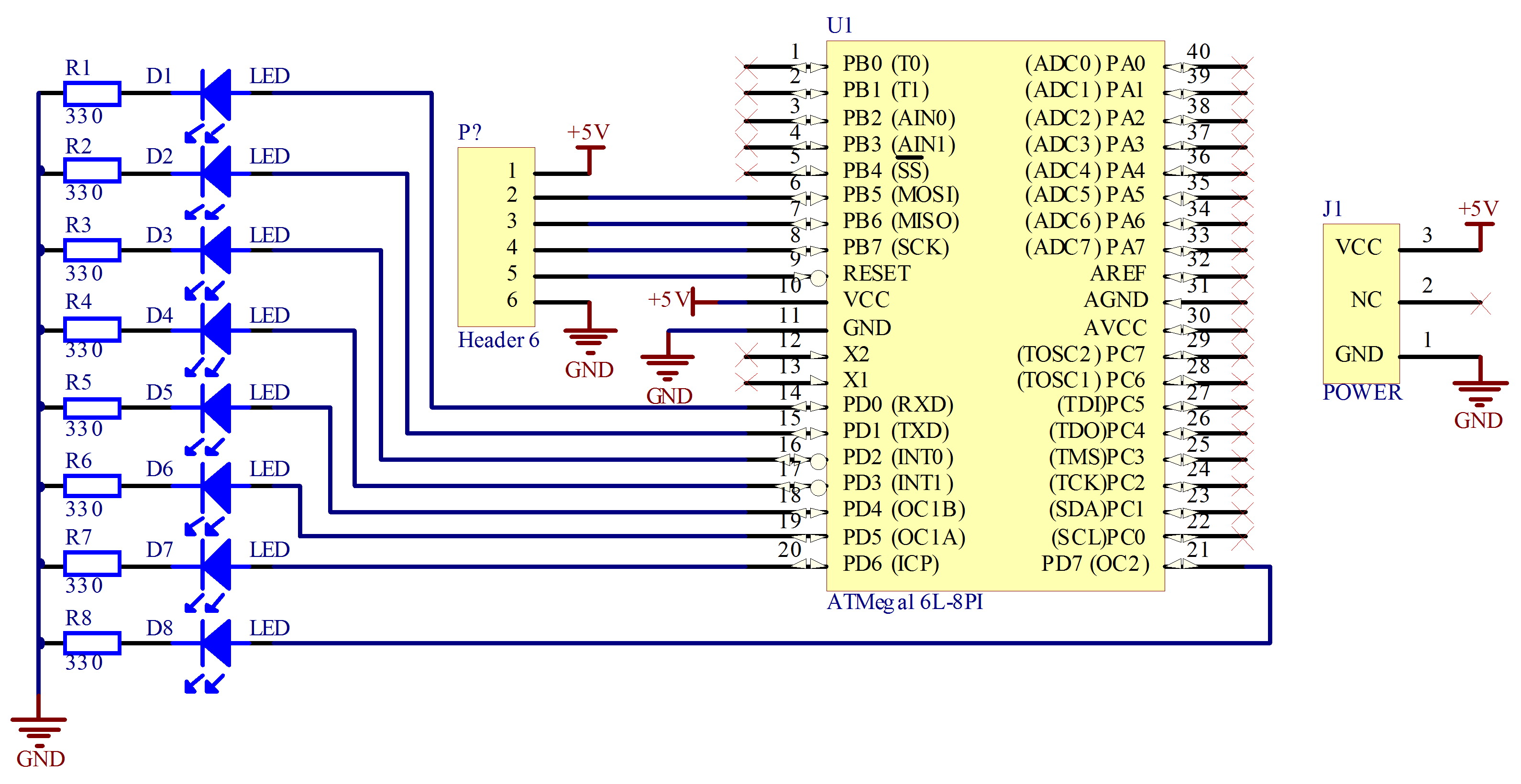
The project involves assembling a circuit that can be completed in 30 minutes. The required parts include: 1 circuit board, 1 Atmel AVR Atmega16 microcontroller, and 8 resistors with a value of 330 ohms each. The schematic for this project...
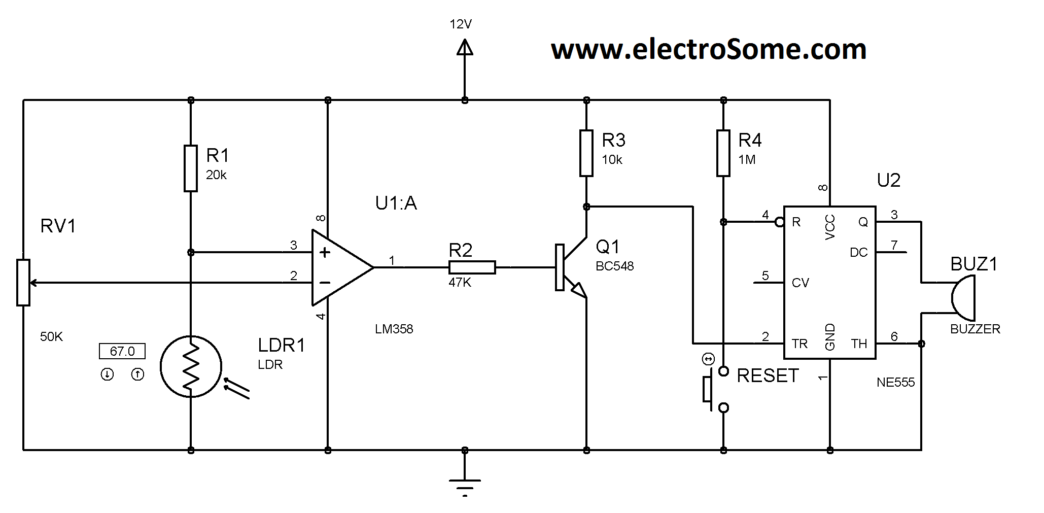
A simple and affordable laser-based security system, costing less than Rs. 100. This circuit utilizes an LM358 operational amplifier and an LM555 timer. It is activated when the laser beam is interrupted by a light-dependent resistor (LDR), which triggers...
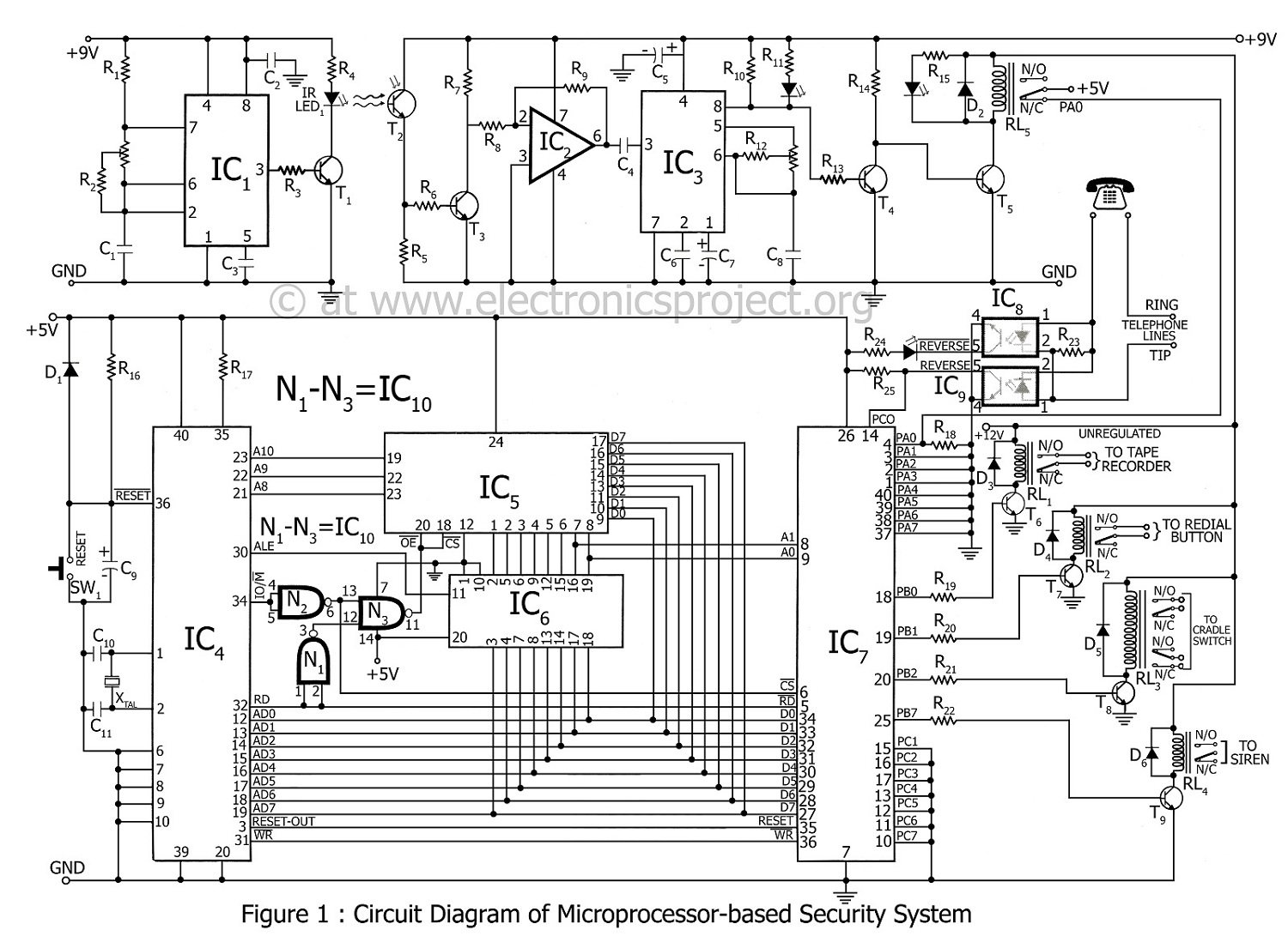
A microprocessor-based home security system project. This advanced security system not only notifies the user but also alerts the police immediately. In the 8085 microprocessor-based home security system, control is exercised over a siren, telephone (via cradle and redial...

The circuit utilizes the MAX8743 chip for a laptop chipset power supply. It demonstrates the conversion of a 5V power supply into +2.5V and +1.8V outputs. The MAX8743 is a highly integrated power management solution designed specifically for laptop chipsets....

We have developed a powerful yet inexpensive and easy to construct experiment control system. The construction of the system together with the control software is described here. All circuits and software are free to download and use for nonprofit....
This text discusses the MSC1210 microcontroller as the core of a high-accuracy temperature measurement system, which includes signal processing and communication capabilities. The system is designed for easy expansion, allowing for accurate measurements and fast data acquisition. The hardware...