
Data collecting system of LCD human-computer interaction
The MSC1210Y5 microcontroller serves as the central component of a sophisticated temperature measurement system that integrates signal processing and communication functionalities. The architecture is designed to facilitate high-accuracy data acquisition, making it suitable for applications requiring precise temperature monitoring. The system's modular design allows for easy expansion, enabling the addition of various sensors or interfaces as needed.
The front-end data acquisition module is equipped with an advanced 24-bit ADC, which ensures high-resolution measurements. The integration of a programmable gain amplifier allows the system to adapt to various signal levels, enhancing its versatility in different measurement scenarios. The inclusion of a numerical filtering section further improves data integrity by reducing noise and unwanted artifacts from the acquired signals.
Communication between the front-end and rear-end systems is established via an RS-232 interface, a standard protocol that ensures reliable data transfer. This choice of communication interface simplifies integration with other devices and systems, enhancing the overall functionality of the measurement system.
The low power consumption characteristics of both the MSC1210Y5 and MAX3223 components are crucial for applications where power efficiency is paramount. By operating at a voltage of 3.3V, the system minimizes energy usage while maintaining performance, making it suitable for battery-operated or remote sensing applications.
The design of the circuit includes reserved pathways for future expansions, such as additional serial ports or SPI interfaces, allowing the system to adapt to evolving application requirements. This foresight in design enhances the longevity and utility of the measurement system.
The control flow of the data acquisition circuit is meticulously structured to ensure seamless operation. The system's ability to read commands from the upper computer and adjust the ADC settings in real time exemplifies its responsiveness and adaptability. By segmenting the data into three bytes for transmission, the design accommodates the high precision of the ADC, ensuring that the integrity of the temperature measurements is preserved throughout the communication process.
Overall, the MSC1210-based temperature measurement system exemplifies a well-engineered solution for high-accuracy data acquisition, combining advanced microcontroller capabilities with flexible design features suitable for a wide range of applications.This text regards MSC1210 as the cores of measuring, SIGPROC signal processing and communication, has designed the module of acquisition system of high-accuracy temperature. It is easy to expand that this system measures the passway, survey accuracy is high, can carry on the measurement of the high accuracy data fast.
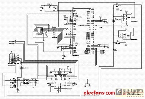
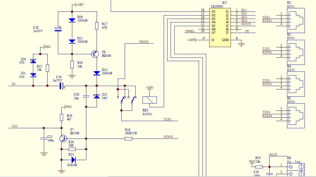
The hardware part of this sys tem is mainly made up of data acquisition of forward end, processing circuitry, rear end data processing, LCD circuit. Two parts carry on communication through RS-232 serial interface. The overall scheme of the system is patterned and shown as in Fig. 1. Data acquisition partial key device chooses MSC1210Y5. This is mainly because this microprocessor has 24 ²s ADC, its available accuracy is higher than 22. Its inside includes the intact forward path including inputting buffer memory, simulation switching circuit, programmable gain amplifier, ADC and numerical filtering part And after in DAC passway, finish not must observe and control these on systematic oning some.
In addition, this processor sets up the internal passway function by way of changing the command register, all right the intersection of selection input and buffer memory, arrangement enlarge gain to noise temperature ratio, control channel switch switch over, go on, bias, correct etc. with order, it is very convenient to use. The partial circuit structure schematic diagram of data acquisition is shown as in Fig. 2. Two are key the power consumption of the chip MSC1210Y5 and MAX3223 is very low in this system, so, the power 3.
3V in designing the moderato Offered through RS-232 interface from the back end system. Except the intersection of RS-232 and interstar connection of interface, insert J1, the intersection of J2 and signal 8 the intersection of AIN and line, and REF publically of socket Outside the line, the hardware part of this system no longer needs other connections, it is very convenient to use. In addition, also reserve some rabbit lines to expand systematic function application in the circuit after supporting while designing, including the second serial port and four can be configured to SPI interface, interrupt input and oral spare rabbit line of I/O end.
In the module of high-accuracy temperature measurement based on this circuit is employed, MSC1210Y5 has finished the multi-channel switch of the small signal, functions such as signal buffering, programming amplifying, 24 ADCs, numerical filtering, data processing, signal normalizing and serial port communication, etc. MSC1210Y5 includes 2 serial ports, chooses a serial port among them used for communicating with the man-machine interacting system of rear ending in this design, control command and control parameter that is responsible for receiving the rear end and sending and data gathered, dealt with of sending the forward end.
The procedure primary service of the data acquisition circuit is: Control the measurement process of internal ADC, read the data changed; And rear end S3C44B0X system Carry on communication, read order and relevant control parameters of the upper computer, convey the data after changing to the upper computer at the same time. The procedure control flow chart of the data acquisition circuit is shown as in Fig. 3. When the serial port begins to receive order and data that the upper computer sends up, the 2 bytes series code of back end system read sequentially have R6 temporarily, R7 Control word be lasted ADCON1 and ADCON0, be thus not realized ADC the loads of the control commands.
Thereafter the internal load corresponding orders and parameter value of ADCON3, ADCON2, ADMUX and PDCON register, thus finish to arrangement and start of ADC in MSC1210Y5. Rearward end system, at the transmission data, because ADC is 24 precision, changing the data must be divided into a 3 bytes conveying, change the result of ADC of the register 1, 2, 3 to send through sending SBUF sequenti
🔗 External reference
Related Circuits
This is a complete alarm system with five independent zones suitable for a small office or home environment. It utilizes three CMOS integrated circuits and features a timed entry/exit zone, four immediate zones, and a panic button. There are...
This circuit utilizes a 16x2 LCD to display a count value using an 8051 microcontroller. The maximum count value is set to 99. The circuit consists of the 8051 microcontroller, a 16x2 LCD, and two switches designated for incrementing...
An alternative approach involves obtaining a motor's counter electromotive force from the motor end of the related signal after it has been amplified and averaged across three pins. The drive output A functions as a single-ended output, which controls...
Create a simple telephone-based intercom system in a new house. Shouting between rooms is not effective, and using an instant messaging client or FaceTime lacks the immediacy of a voice call. A collection of old wired telephones is available...
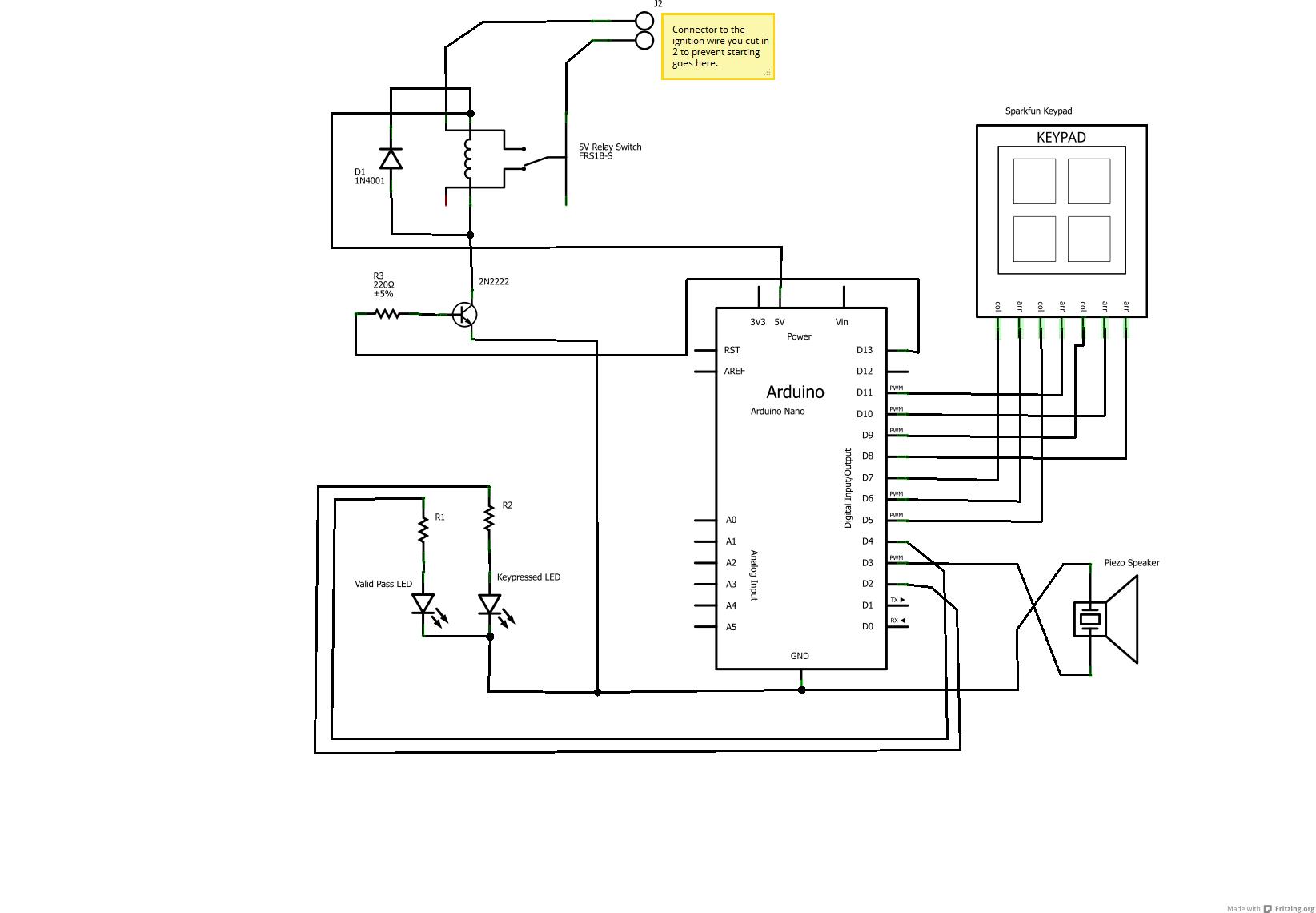
Audible signals will alert if the password or keycode entered is accepted or not (in this case, random sounds for incorrect entries and the Super Mario theme for success) using a standard piezo speaker. The under-dashboard USB hub is...
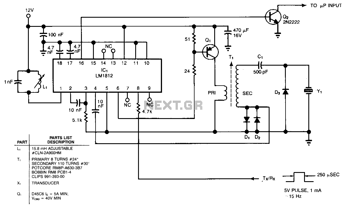
Combine an electrostatic transducer with an ultrasonic transceiver integrated circuit (IC) to create a ranging system capable of sensing objects at distances from 4 inches to over 30 feet. The broadband characteristics of transducer Y1 simplify the tuning process....