
The 555 Monostable
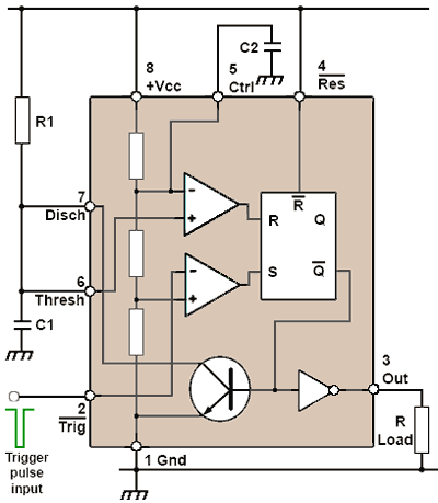
The 555 timer in monostable mode is a versatile component widely used in timing applications. Its operation is based on the interaction between the timing capacitor and resistor, which define the output pulse duration. When the circuit is initially powered, the output is low, and the timing capacitor is discharged. A trigger pulse applied to pin 2 must be a brief dip below 1/3Vcc to initiate the timing cycle. This pulse causes the internal flip-flop of the timer to set, switching the output to high and allowing the capacitor to begin charging through the resistor R1.
The voltage across the capacitor increases exponentially, and the time taken to reach 2/3Vcc is critical for determining the duration of the output pulse. The relationship between the resistor, capacitor, and the output pulse duration can be expressed as T = 1.1 * R1 * C1, where T is the time duration for which the output remains high. The choice of resistor and capacitor values is essential. For accurate timing, R1 should generally be between 1KΩ and 1MΩ, while C1 should be selected with consideration for leakage and tolerance characteristics.
The circuit design also incorporates decoupling capacitors (C3 and C4) to mitigate external noise, ensuring stable operation. A common practice is to use a 100nF ceramic capacitor for high-frequency noise and an electrolytic capacitor of around 2µF for low-frequency noise, both placed close to the 555 IC.
For applications requiring very short output pulses, it is advisable to avoid using capacitors below 100pF due to the influence of stray capacitance. Furthermore, when using electrolytic capacitors, attention must be paid to their polarity to prevent damage and ensure proper functionality. In cases where longer timing intervals are needed, cascading multiple 555 timers or utilizing digital counters can provide a more reliable solution.
The 555 timer is an essential component in various electronic applications, from simple timers to complex pulse generators, showcasing its adaptability and effectiveness in timing and control systems.The 555 timer is so named because its primary mode of operation is intended to be in monostable mode. Operating as a monostable, it does not fit the strict definition of an oscillator because, unlike true oscillators, it requires an input signal to trigger its operation, however the fact that the 555 timer can be used in both monostable and astabl
e mode considerably increases its flexibility and usefulness. Unlike the astable, which has two unstable states and so continually switches from one to the other and back again, the monstable has one stable state and one unstable state. When triggered by a suitable pulse at its input (pin 2) it switches from its stable state, in which the output is low, to its unstable state where its output is high.
This state exists for a time controlled by the values of R1 and C1, and at the end of this period the output switches back to its stable (low) state. Its primary use is therefore to produce a set time delay, initiated by an input pulse. From Fig. 4. 5. 1 it can be seen that the circuit differs from the basic astable configuration shown in Oscillators Module 4.
3 in that only one timing resistor (R1) is used, pins 6 and 7 (instead of 6 and 2) are connected together and pin 2 is used for the trigger pulse input. Fig. 4. 5. 2 illustrates the timing waveforms for the monostable, notice that the trigger pulse on pin 2, which must be higher than 1/3Vcc in the absence of a trigger pulse but is normally at about +Vcc, falls to less than 1/3 Vcc to trigger the start of the delay (high output) period.
The trigger pulse makes the voltage on the inverting input of comparator 2 lower than its non-inverting input and so the comparator output goes high, making the S input of the bistable high and setting the bistable Q output high, and its Q (not Q) output low. This turns off the discharge transistor and the low output from the bistable is inverted by the inverter to make the output at pin 3 high.
C1 commences charging from 0V towards +Vcc, but once VC1 reaches the discharge level of 2/3Vcc, Comparator 1 is triggered, the bistable is reset, the output at pin 3 goes low and the discharge transistor immediately discharges C1. As C1 is also connected to the non-inverting input of comparator 2, this voltage also falls, and as the trigger voltage on pin 2 is now high again after the trigger pulse, the 1/3Vcc threshold level that was active in the astable configuration is ignored as VC1 falls and C1 is fully discharged to 0V.
No further action takes place until the arrival of a further trigger pulse at pin 2, and during this time the monostable is said to be in its stable state. Fig. 4. 5. 3 shows a schematic diagram for a basic 555 monostable circuit with an output pulse duration of just over 1 second.
Because this circuit is not working at high frequencies, the supply decoupling capacitors C3 and C4 may be considered as optional, but nevertheless it is good practice to make sure the circuit is not affected by external noise by decoupling the 555 supply with a 100nF capacitor (to remove high frequency noise) and an electrolytic of around 2 F (to remove low frequency noise). Both of these capacitors should be fitted as physically close to the 555 IC as possible. In monstable mode, only one resistor and one capacitor are involved in the timing process, and as the capacitor charges from 0V to 2/3Vcc in 1.
1 time constants, from the information on capacitor time constants, a capacitor will charge in an exponential fashion to 63. 2% of its full charge voltage (+Vcc) in one time constant, so to reach 2/3Vcc (66. 7%) will take 1. 1 time constants. The delay period (T) is the time taken for the timing capacitor to charge to this level and so can be simply calculated as: As the point at which the capacitor begins to discharge is a fraction (2/3) of Vcc, due to the internal resistor chain in the 555, waveform timing is unaffected by changes in the supply voltage.
The 555 monostable can generate delays from a few microseconds to several hours depending on the values or R1 and C1. However, using very large capacitor values can be a problem, since large value electrolytic capacitors have quite wide tolerance limits, so their actual value may not be the same as their value markings by a significant amount.
They also have high leakage currents and this can affect the timing accuracy as the capacitor charges. Where large capacitance values must be used, tantalum capacitors can be a better choice due their lower leakage current.
High working voltage electrolytic capacitors should also be avoided where possible as electrolytics do not function properly as capacitors when operated at voltages less than about 10% of their rated working voltage. For example, using an electrolytic capacitor rated at 100Vwkg in a 555 circuit operating on a 5V supply could also cause timing problems.
Capacitor working voltages should therefore be chosen that are higher than the 555 +Vcc voltage, so that they can work safely without the danger of an over voltage causing a sudden and catastrophic short circuit in the capacitor, but not so high that they cause timing problems. Very small value timing capacitors used in producing very short output pulses may also cause problems.
If values below 100pF are used, stray capacitance around the circuit can change the value of timing capacitance considerably, leading to inaccurate and unpredictable timing. WARNING: Be extra careful when connecting electrolytic capacitors to ensure they are connected with the correct polarity, see Fig.
4. 5. 4 showing negative lead marking on a capacitor, but note that the convention for capacitor symbols in circuit schematic diagrams (e. g. Fig. 4. 5. 3) is to mark the positive plate of an electrolytic capacitor with a + symbol. Fig. 4. 5. 4 also shows the safe working voltage of the capacitor, which must be high enough to withstand any likely voltage the capacitor will be subject to in the circuit.
As with astables, the timing resistor must be at least 1K © (and higher is better if low power consumption is an aim), but if timing inaccuracies are to be minimised, it should not be much higher than 1M ©. If timing delays are needed that are longer than can be accommodated by following the above information, it is possible to use multiple monostables, with the falling output of one triggering the next.
However an even better (and possibly cheaper) option would be to use digital counters for timing purposes. To trigger the 555, pin 2 must momentarily go to less than 1/3Vcc, the duration of the trigger pulse must not be longer than that of the output pulse, and with short output periods or long duration input (trigger) pulses, some conditioning of the trigger pulse may be needed to keep its duration short.
A common method is to differentiate the trigger pulse to produce a very narrow negative going spike at the falling edge of the pulse as shown in Fig. 4. 5. 5. The differentiator Cd and Rd produces two spikes symmetrical about +Vcc, but as spikes going more positive than +Vcc will not play any part in triggering the 555 and would additionally contribute to unwanted noise in the circuit, they are removed by D1, which will prevent any voltages higher than +Vcc appearing at pin 2.
The result is a much narrower trigger pulse, the duration of which will depend on the values of Rd and Cd. The values of these components are not critical provided that Rd does not load the input too much and reduce the amplitude of the trigger pulse, and that the resulting duration of the trigger pulse (at 1/3Vcc) is less than the duration of the output pulse.
🔗 External reference
Related Circuits
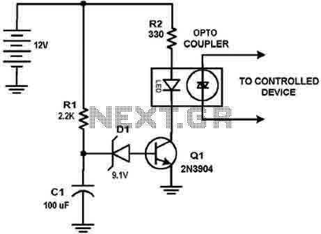
This circuit design was used to switch on device via a LED photocell arrangement (optocoupler) using components R1, C1, D1 and Q1. It produces a delay on powering up to ensure correct sequencing of certain equipment. A very simple...
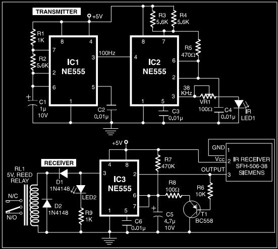
This post discusses a proximity detector circuit primarily utilizing the NE555 integrated circuit (IC). The circuit is designed for burglar alarms based on beam interruption, with the advantage that the transmitter and receiver are contained within the same enclosure,...

The transistor characteristic curve tracer circuit depicted in Figure 555 illustrates the characteristics of a transistor. It utilizes two voltages: a step wave applied to the base (b) to generate different base currents (Ib), and a sawtooth waveform at...

VDI, VD2, C3, and C4 form a simple half-wave rectifier capacitor step-down regulator circuit. This circuit can output approximately 12V DC voltage after power is applied across C3, which is utilized for the time base circuit. Additionally, the time...
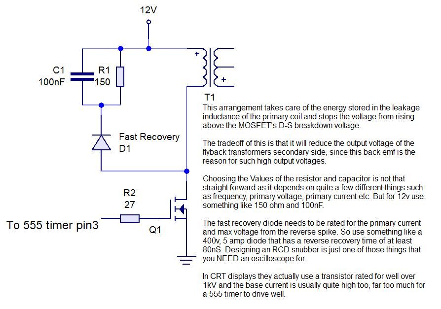
This instructable demonstrates the process of creating an audio-modulated plasma speaker using a flyback transformer salvaged from an old CRT display. The audio-modulated plasma speaker operates by utilizing a high-voltage output from a flyback transformer to create a plasma arc...
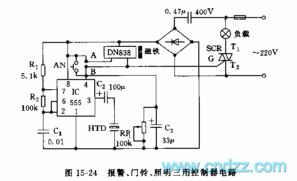
The controller circuit illustrated in Figure 15-24 consists of a switch-type Hall integrated circuit DN838 and an astable multivibrator, which is based on the 555 timer IC. This circuit is suitable for various applications, including automatic door opening, delay...