

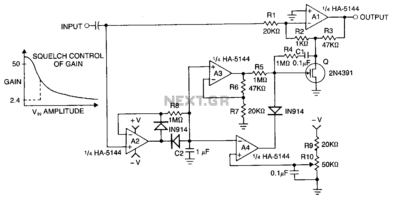

Agc-with-squelch-control
Automatic gain control is a very useful feature in a number of audio amplifier circuits: tape recorders, telephone speaker phones, communication systems and PA...
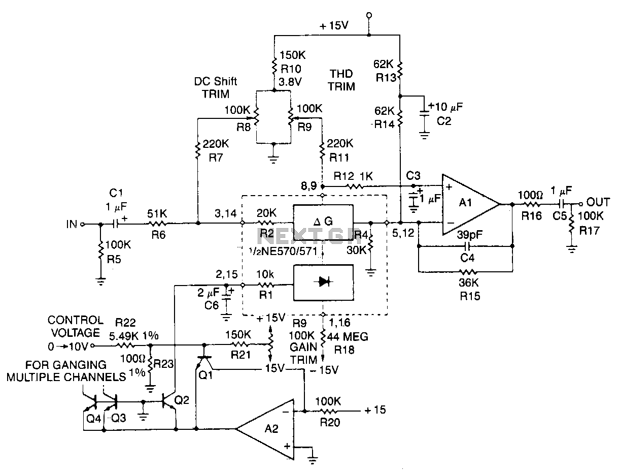
Voltage-controlled-attenuator
This typical circuit uses an external op amp for better perlormance and an exponential converter to get a control characteristic of -6 dB IV. Trim networks are...
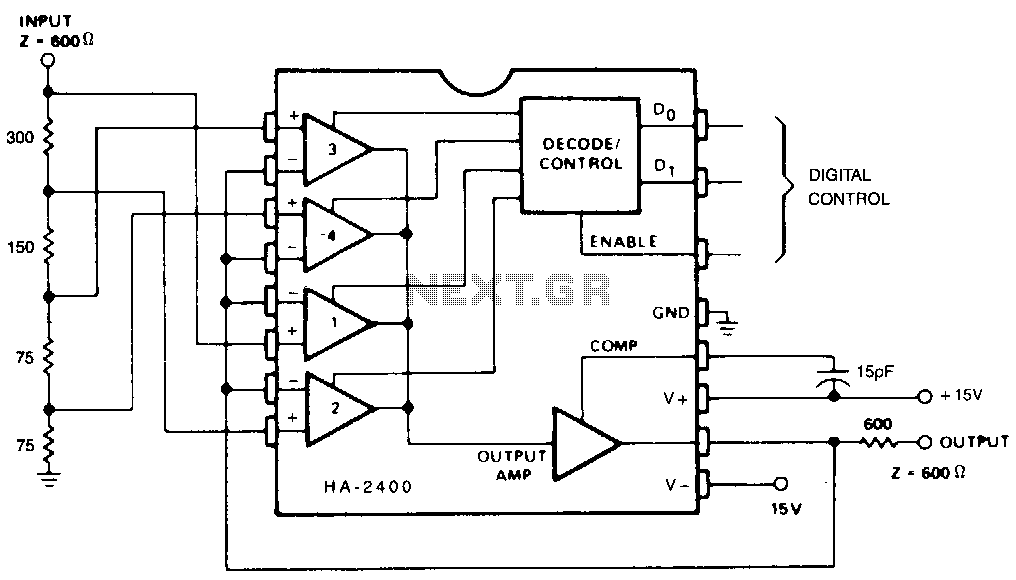
Programmable-attenuator
This circuit performs the function of dividing the input signal by a selected constant (1, 2, 4, 8, etc.). While T, Z, or L sections could be used in the input...
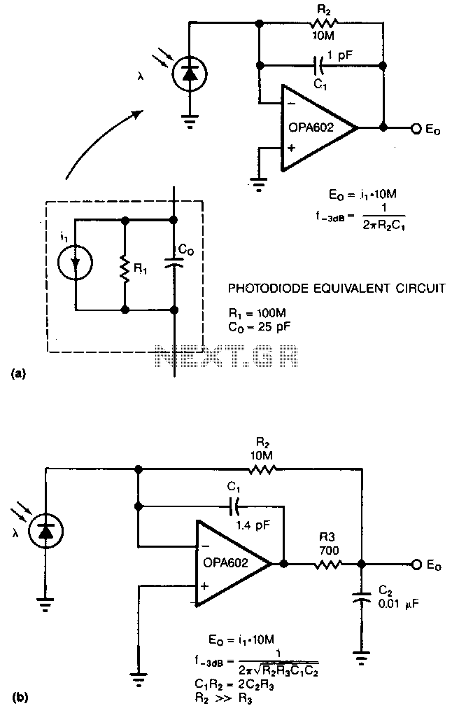
Photodiode-amplifier
Adding two passive components to a standard photodiode amplifier reduces noise. Without the modification, the shunt capacitance of the photodiode reacting with ...
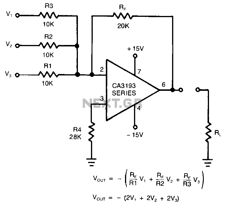
Summing-amplifier
This circuit uses a CA3193 BiMOS op amp. Because input noise of the amplifier is increased by Rp/ Rl//R2/ /R3, and the gain that a single input will amplify is...
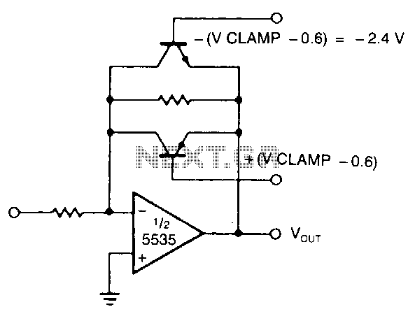
Active-limiting-amplifier
The modified inverting amplifier uses an active clamp to limit the output swing with precision. Allowance must be made for the V8E of the transistors. The sw...
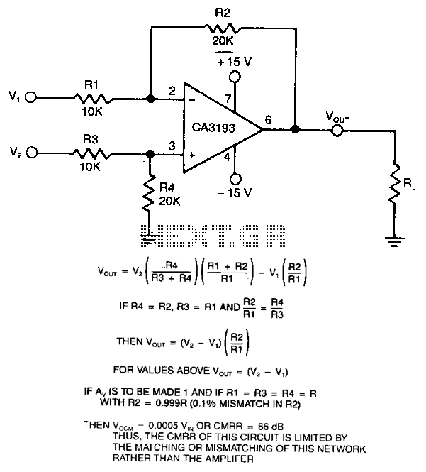
Differential-amplifier
This differential amplifier uses a CA3193 BiMOS op amp. This classical, differential input-tosignal- ended output converter when used with lowresistance signal ...
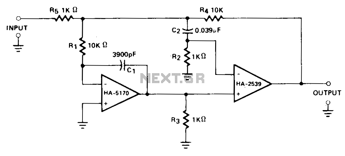
Composite-amplifier
A composite configuration greatly reduces de errors without compromising the high-speed, wideband characteristics of HA-2539. The HA-2540 could also be used, b...
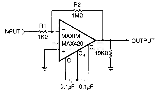
15V-chopper-amplifier
This simple circuit is a gain-of-1000 inverting amplifier. It will amplify submillivolt signals up to signal levels suitable for further processing. In almos...
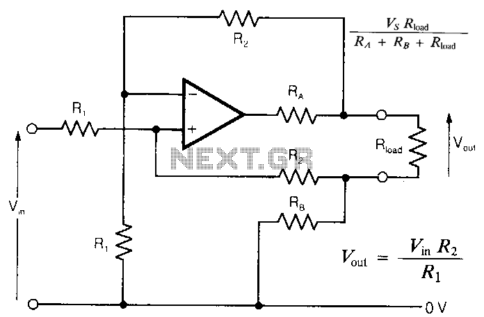
Safe-opamp-circuit
In intrinsically safe applications, it is sometimes necessary to separate sections of circuitry by resistors which limit current under fault conditions. The ci...
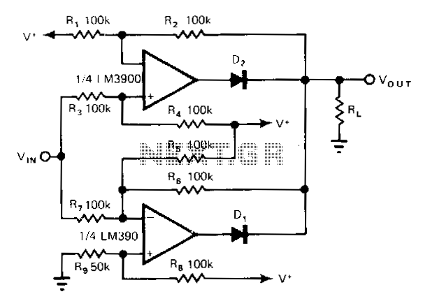
Norton-amplifier
The noninverting amplifier has a gain of R2/R3 (1 in this case) and produces a voltage of V,"" during a positive excursion of Vin with respect to ground. The...
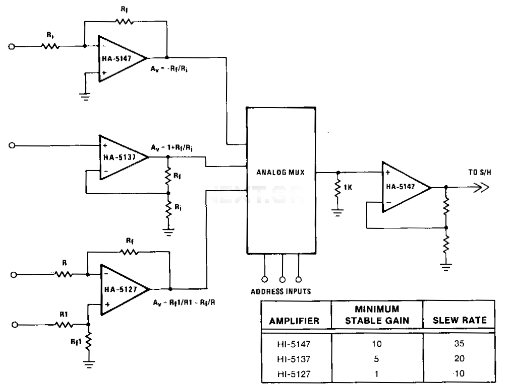
Buffer-amplifier-for-multiplexers
The precision input characteristics of the HA-5147 help simplify system error budgets, while its speed and drive capabilities provide fast charging of the mult...
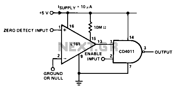
Zero crossing detector
This detector is useful in sine wave squaring circuits and A/D converters. The positive input may either be grounded or con-output nected a nulling voltage whic...
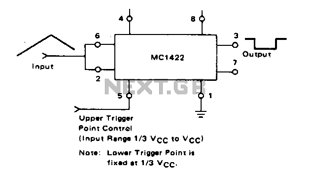
Schmitt trigger
The lower trigger point is fixed at % Vcc, but the upper trigger point is adjustable by means of Pin 5 from Vi Vcc to slightly less than Vcc...
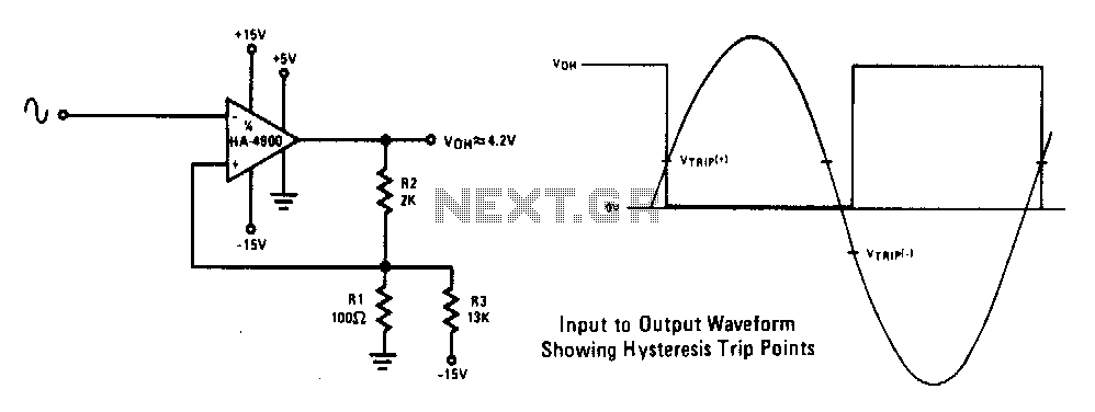
Schmitt trigger zero crossing detector
This circuit has a 100 mV hysteresis which can be used in applications where very fast transition times are required at the output even though the signal is ver...
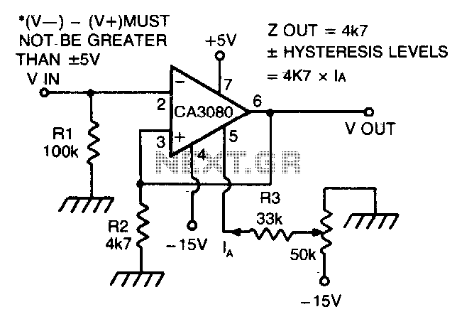
Schmitt trigger with programmable hysteresis
CA 3088 is used as a versatile Schmitt trigger. The size of the hysteresis levels is determined by Ia that flows out of the amplifier"s output and through R2. I...

Schmitt trigger
By replacing the common-emitter resistor in a conventional Schmitt by a zener diode...
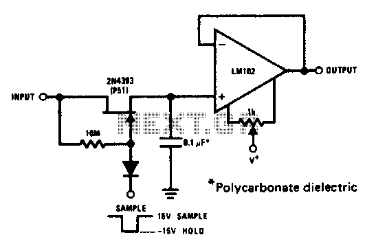
Sample and hold
The 2N4393 JFET was selected because of its low less (< 100 pA), very low ID (< 100 pA) and low pinchoff voltage...
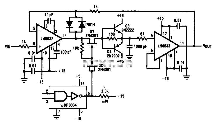
High speed sample and hold
This circuit exhibits a 10 V acquisition time of 900 ns to 0% accuracy and a droop rate of only 100 µ-V/ms at 25° C ambient condition. An even faster acqu...
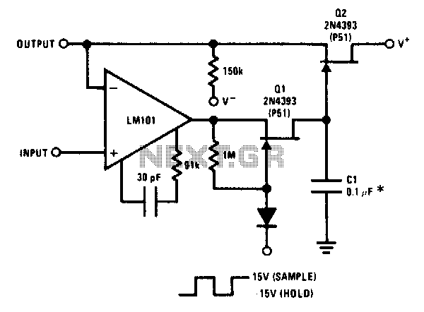
Sample and hold
The JFETs, Ql and Q2, provide complete buffering to Cl, the sample and hold capacitor. During sample, Ql is turned on and provides a path, rds(on), for charging...