


Mixing analog multiplier integrated circuit MC1496
#analog multiplier
#MC1496
#balanced modulator
#communications receiver
#diode ring mixer
#differential pair
#RF mixer
#signal processing
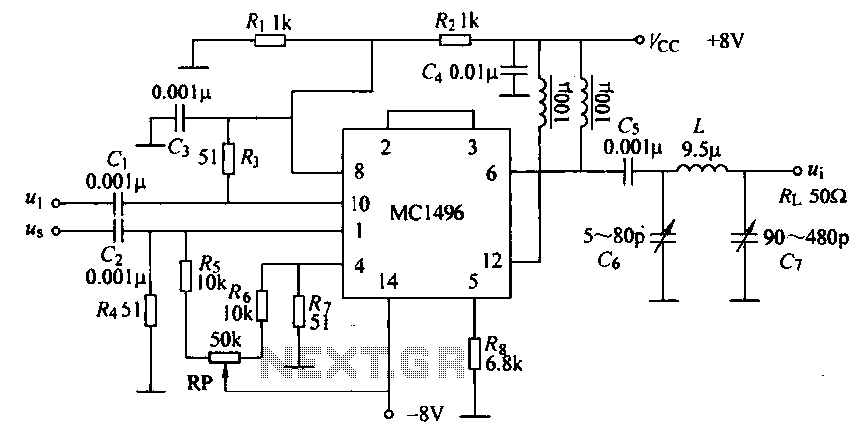
Description: Currently, a high-quality communications receiver utilizes diode ring mixers and a double differential pair balanced modulator, configured as an analog multiplier (MC1496). The mixer circuits are illustrated in the accompanying figure. The local oscillator (LO) voltage and the input signal voltage from the input channel hoppers are adjusted using a 50 kΩ potentiometer, while a foot DC potentiometer is used for zeroing. This setup not only influences the mixer input signal voltage and the local oscillator voltage but also accounts for the presence of interference and noise signals. The interaction between any two of these signals may produce a combined frequency. If the frequency of the combined signal is equal to or close to the intermediate frequency, the input signal will pass through an intermediate frequency amplifier and a demodulator, leading to an output stage that generates interference. The most significant impacts arise from intermediate frequency interference and mirror interference. The intermediate frequency (IF) signal, operating at 9 MHz, is extracted from the single-ended output after being processed through a bandpass filter.
The described communications receiver employs advanced mixing techniques to ensure high fidelity in signal processing. The diode ring mixer is essential for its ability to efficiently combine signals, while the double differential pair balanced modulator enhances linearity and minimizes distortion. The MC1496 analog multiplier serves as the core component for mixing, allowing for precise control over modulation and demodulation processes.
The configuration of the 50 kΩ potentiometer plays a critical role in fine-tuning the local oscillator voltage and input signal voltage, which are pivotal for optimizing the receiver's performance. The foot DC potentiometer is employed to establish a zero reference point, ensuring that any potential DC offsets do not adversely affect the signal integrity.
Interference and noise signals can significantly degrade the quality of the received signal. The design anticipates these challenges by allowing for adjustments that help mitigate their impact. The combined frequency generated by the interaction of the input and local oscillator signals can lead to unwanted frequency components. If these components align with the intermediate frequency, they can introduce additional noise into the system.
The intermediate frequency amplifier is tasked with amplifying the desired signal while filtering out unwanted frequencies. The subsequent demodulator processes this amplified signal, preparing it for output. The output stage is crucial, as it must deliver a clean signal while minimizing interference. The primary concern is the intermediate frequency interference and mirror interference, which can distort the demodulated output.
Finally, the extraction of the 9 MHz IF signal from the single-ended output is accomplished using a bandpass filter, which selectively allows the desired frequency to pass while attenuating others. This filtering step is essential for maintaining the integrity of the received signal, ensuring that the output is as clear and accurate as possible. The overall design reflects a sophisticated approach to high-quality communication receiver architecture, addressing the complexities of signal mixing and interference management.Currently, high-quality communications receiver in the use of diode ring mixers and mixer by a double differential pair balanced modulator constituted, set into an analog multiplier (MC1496) shown in Figure mixer circuits. LO voltage HL and the input signal voltage input from the input channel hoppers were adjusted 50kfl potentiometer, O, foot DC potentiometer zero. In addition to acting on the mixer input signal voltage and the local oscillator voltage Sapporo soul, but also the presence of interference and noise signals.
Between any two of them are likely to produce the combined frequency, if the frequency of the combined signal is equal to or close to an intermediate frequency, the input signal - in time through intermediate frequency amplifier, a demodulator, the output stage produces interference, the influence of the received signal, inevitably to cause interference, in which the greatest impact is the intermediate frequency interference and interference mirror. IF signal (9MHz) removed from the single-ended output foot after Ji bandpass filter.
The described communications receiver employs advanced mixing techniques to ensure high fidelity in signal processing. The diode ring mixer is essential for its ability to efficiently combine signals, while the double differential pair balanced modulator enhances linearity and minimizes distortion. The MC1496 analog multiplier serves as the core component for mixing, allowing for precise control over modulation and demodulation processes.
The configuration of the 50 kΩ potentiometer plays a critical role in fine-tuning the local oscillator voltage and input signal voltage, which are pivotal for optimizing the receiver's performance. The foot DC potentiometer is employed to establish a zero reference point, ensuring that any potential DC offsets do not adversely affect the signal integrity.
Interference and noise signals can significantly degrade the quality of the received signal. The design anticipates these challenges by allowing for adjustments that help mitigate their impact. The combined frequency generated by the interaction of the input and local oscillator signals can lead to unwanted frequency components. If these components align with the intermediate frequency, they can introduce additional noise into the system.
The intermediate frequency amplifier is tasked with amplifying the desired signal while filtering out unwanted frequencies. The subsequent demodulator processes this amplified signal, preparing it for output. The output stage is crucial, as it must deliver a clean signal while minimizing interference. The primary concern is the intermediate frequency interference and mirror interference, which can distort the demodulated output.
Finally, the extraction of the 9 MHz IF signal from the single-ended output is accomplished using a bandpass filter, which selectively allows the desired frequency to pass while attenuating others. This filtering step is essential for maintaining the integrity of the received signal, ensuring that the output is as clear and accurate as possible. The overall design reflects a sophisticated approach to high-quality communication receiver architecture, addressing the complexities of signal mixing and interference management.Currently, high-quality communications receiver in the use of diode ring mixers and mixer by a double differential pair balanced modulator constituted, set into an analog multiplier (MC1496) shown in Figure mixer circuits. LO voltage HL and the input signal voltage input from the input channel hoppers were adjusted 50kfl potentiometer, O, foot DC potentiometer zero. In addition to acting on the mixer input signal voltage and the local oscillator voltage Sapporo soul, but also the presence of interference and noise signals.
Between any two of them are likely to produce the combined frequency, if the frequency of the combined signal is equal to or close to an intermediate frequency, the input signal - in time through intermediate frequency amplifier, a demodulator, the output stage produces interference, the influence of the received signal, inevitably to cause interference, in which the greatest impact is the intermediate frequency interference and interference mirror. IF signal (9MHz) removed from the single-ended output foot after Ji bandpass filter.
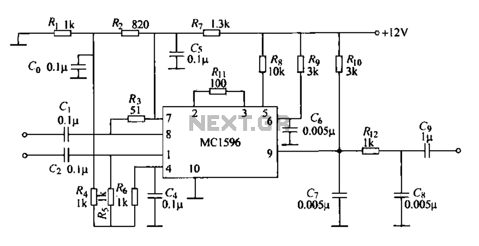
Consisting of integrated analog multiplier MC1596 synchronous detector
The circuit features an integrated analog multiplier, the MC1596, functioning as a synchronous detector. It is designed to demodulate amplitude-modulated signals sourced from an integrated circuit. The output signal is derived from the O pin, where a local carrier frequency...
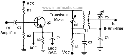
RF Mixer Circuit
In general terms, a mixer is any circuit that combines two or more circuits or signals into a common output. A more specific definition describes a mixer as a nonlinear circuit that accepts two different frequencies (F1 and F2) as...
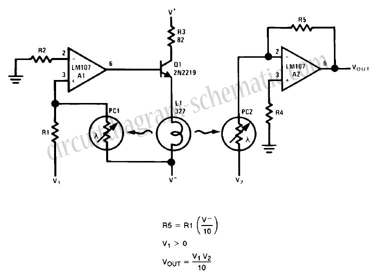
Simple Analog Multiplier Circuit Using LM107
This circuit is a simple analog multiplier. The operation of the circuit can be understood by considering A2 as a controlled gain amplifier that amplifies V2, with its gain dependent on the ratio of the resistance of PC2 to R5....
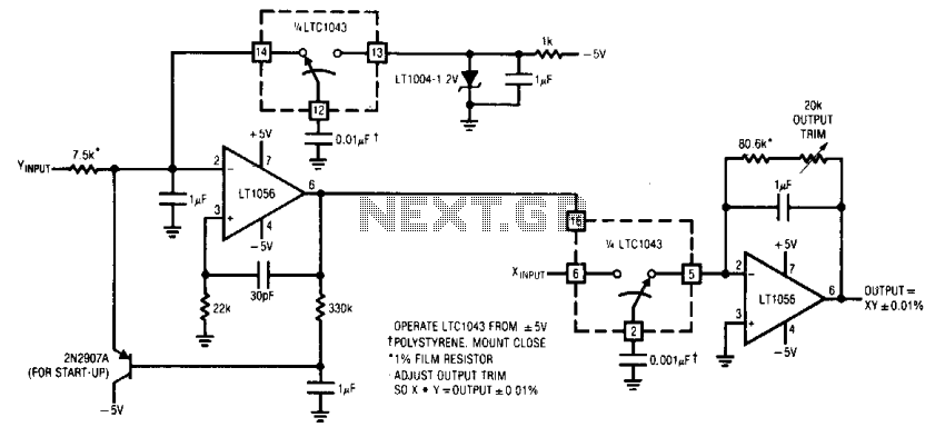
Analog multiplier
The F-V input frequency is locked to the V-F output because the LTCIG43's clock is common to both sections. The F-V's reference is used as one input of the multiplier, while the V-F provides the other. To calibrate, short the...
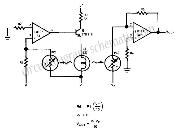
Simple Analog Multiplier Circuit Using LM107
This circuit is a simple analog multiplier. The operation of the circuit can be understood by considering A2 as a controlled gain amplifier. It involves components such as an analog multiplier, a log-antilog circuit, and a summing junction, along with...
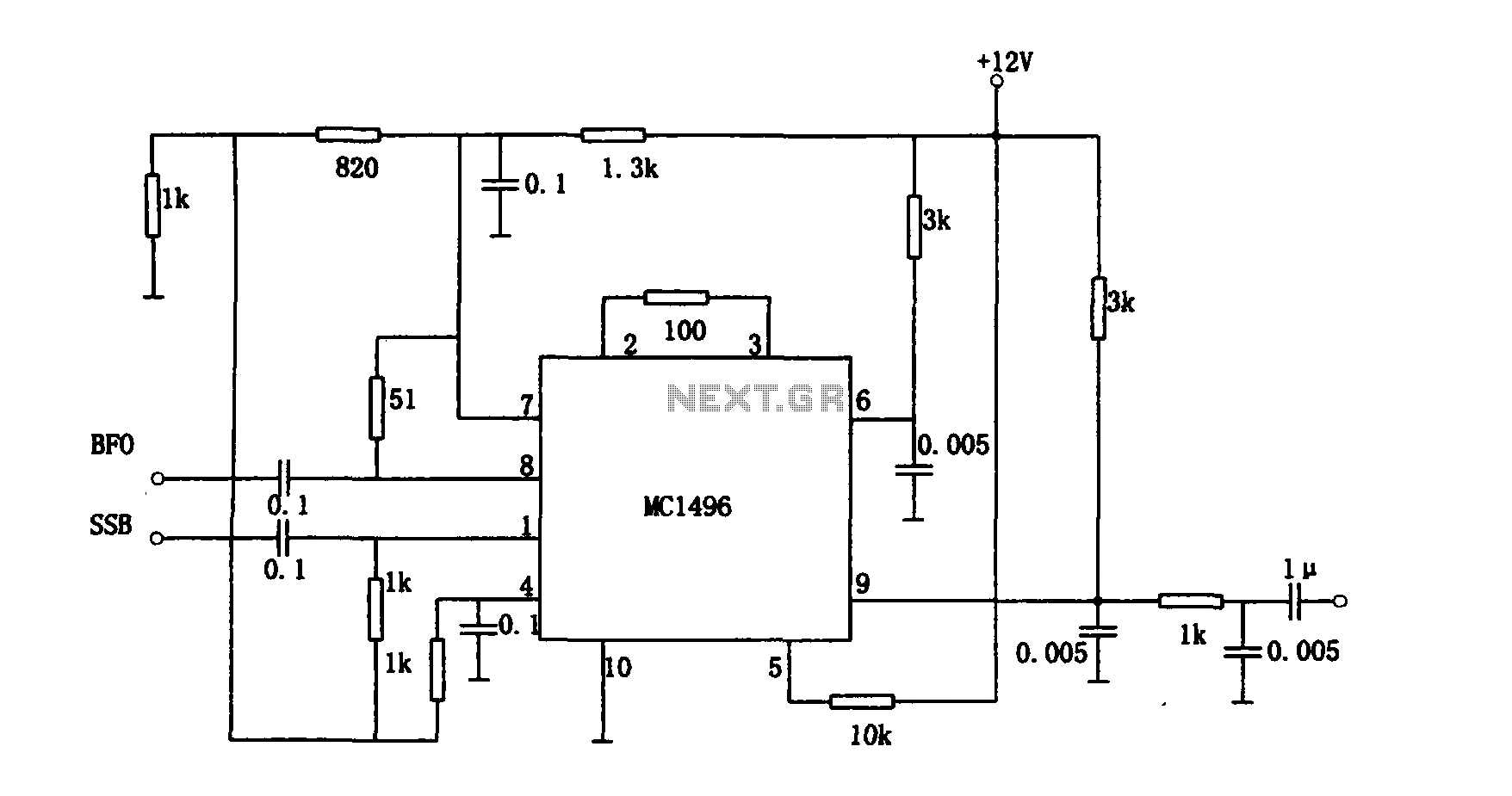
Multiplication detector circuit with MC1496
The provided information pertains to a detector circuit designed for multiplication. This circuit functions as a single-sideband amplitude modulation (SSB AM) signal detector, utilizing its principles to demodulate the received single-sideband signal and recover the transmitted signal. It employs carrier...
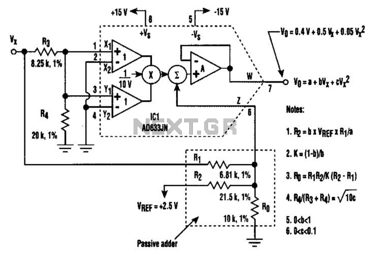
Second-Order Polynomial Generator Circuit
A circuit utilizing a single analog multiplier and five precision resistors can produce an output voltage (Ko) that represents a second-order polynomial. This circuit implements the quadratic function. The input terminals of IC1 are configured to create a positive square...
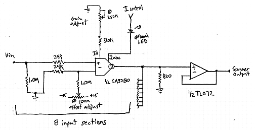
Interpolating Scanner Circuit
This design is for an interpolating scanner, a circuit featuring multiple signal inputs, a control voltage input, and a signal output. The output selectively transitions between inputs, smoothly fading from one to the next as the control voltage increases. A...