
Class B audio amplifier
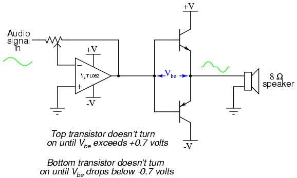
The audio amplifier circuit described is designed to deliver effective amplification for various audio sources while minimizing distortion and maximizing efficiency. The choice of closely matched transistors, specifically the TIP41 and TIP42, is crucial for achieving optimal performance, as their characteristics complement each other, resulting in improved linearity and reduced distortion. The circuit's class B configuration allows for efficient power usage, as each transistor only conducts during half of the waveform cycle. This design choice, while effective, necessitates careful attention to the synchronization of the transistors to avoid crossover distortion, which can degrade sound quality.
To implement this circuit, a power supply capable of providing the necessary voltage and current ratings for the TIP transistors is essential. The circuit should also include appropriate biasing resistors to set the operating point of the transistors, ensuring they operate within their optimal range. Additionally, capacitors may be used for coupling and decoupling purposes to maintain signal integrity and prevent unwanted feedback within the system.
When constructing the amplifier, attention must be paid to the layout and thermal management. Although the circuit can operate without heat sinks, it is advisable to monitor the temperature of the transistors under load conditions to prevent thermal runaway and ensure reliability. Proper grounding and shielding techniques should also be employed to minimize noise and interference, further enhancing the audio quality of the amplified output.
In summary, this audio amplifier circuit represents a practical solution for enhancing audio signals from various sources. By utilizing a class B push-pull configuration with matched transistors, it effectively balances power efficiency and sound quality, making it suitable for both casual listening and more demanding audio applications.The closer matched the two transistors are, the better. If possible, try to obtain TIP41 and TIP42 transistors, which are closely matched NPN and PNP power transistors with dissipation ratings of 65 watts each. If you cannot get a TIP41 NPN transistor, the TIP3055 (available from Radio Shack) is a good substitute.
Do not use very large (i. e. TO-3 case) power transistors, as the op-amp may have trouble driving enough current to their bases for good operation. This project is an audio amplifier suitable for amplifying the output signal from a small radio, tape player, CD player, or any other source of audio signals.
For stereo operation, two identical amplifiers must be built, one for the left channel and other for the right channel. To obtain an input signal for this amplifier to amplify, just connect it to the output of a radio or other audio device like this: This amplifier circuit also works well in amplifying "line-level" audio signals from high-quality, modular stereo components.
It provides a surprising amount of sound power when played through a large speaker, and may be run without heat sinks on the transistors (though you should experiment with it a bit before deciding to forego heat sinks, as the power dissipation varies according to the type of speaker used). The goal of any amplifier circuit is to reproduce the input waveshape as accurately as possible. Perfect reproduction is impossible, of course, and any differences between the output and input waveshapes is known as distortion.
In an audio amplifier, distortion may cause unpleasant tones to be superimposed on the true sound. There are many different configurations of audio amplifier circuitry, each with its own advantages and disadvantages. This particular circuit is called a "class B, " push-pull circuit. Most audio "power" amplifiers use a class B configuration, where one transistor provides power to the load during one-half of the waveform cycle (it pushes) and a second transistor provides power to the load for the other half of the cycle (it pulls).
In this scheme, neither transistor remains "on" for the entire cycle, giving each one a time to "rest" and cool during the waveform cycle. This makes for a power-efficient amplifier circuit, but leads to a distinct type of nonlinearity known as "crossover distortion.
" If the "hand-off" between the two transistors is not precisely synchronized, though, the amplifier`s output waveform may look something like this instead of a pure sine wave: Here, distortion results from the fact that there is a delay between the time one transistor turns off and the other transistor turns on. This type of distortion, where the waveform "flattens" at the crossover point between positive and negative half-cycles, is called crossover distortion.
One common method of mitigating crossover distortion is to bias the transistors so that their turn-on/turn-off points actually overlap, so that both transistors are in a state of conduction for a brief moment during the crossover period: This form of amplification is technically known as class AB rather than class B, because each transistor is "on" for more than 50% of the time during a complete waveform cycle. The disadvantage to doing this, though, is increased power consumption of the amplifier circuit, because during the moments of time where both transistors are conducting, there is current conducted through the transistors that is not going through the load, but is merely being "shorted" from one power supply rail to the other (from -V to +V).
Not only is this a waste of energy, but it dissipates more heat energy in the transistors. When transistors increase in temperature, their characteristics change (Vbe forward voltage drop, ², junction resistances, etc. ), making proper biasing difficult. In this experiment, the transistors operate in pure class B mode. That is, they are never conducting at the same time. This saves 🔗 External reference
Related Circuits
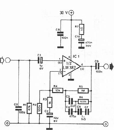
A dynamic microphone preamplifier can be constructed using the LM387 dual operational amplifier integrated circuit. The input impedance is approximately 47k ohms, primarily determined by resistor R1. If a dynamic microphone with a different impedance is to be connected,...
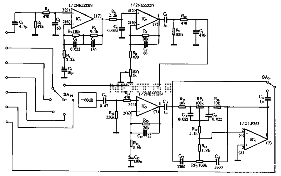
The circuit depicted involves a main amplifier balanced by an electromagnetic pickup, line amplifiers, and a high tone control circuit. It includes components for an electromagnetic player, radio tuner, tape playback, and line input. The preamplifier utilizes an NE5532...
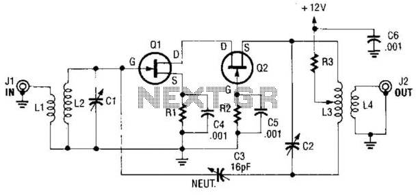
A cascode amplifier using two MOSFETs is illustrated in the diagram. L2C1 and L3C2 resonate at the operating frequency. The circuit offers advantages such as high gain, low noise figure (NF), and excellent linearity. Q1 and Q2 can be...
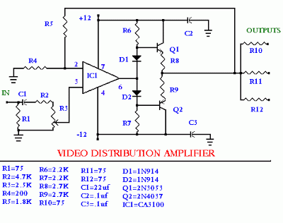
Given the variety of equipment in modern home entertainment systems, the ability to adjust the gain of both audio and video signals has become essential. This particular circuit has proven to be very useful when used alongside the General...
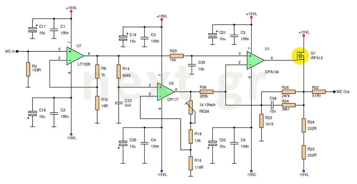
This microphone preamplifier circuit enhances the acoustic signal of a moving coil microphone (MC) with a sensitivity of 150μV at line level. In this design, a specific technique is not employed because the noise produced does not significantly impact...

An audio filter is positioned at the input of each audio integrated circuit (IC) chip to filter the audio signal intended for speakers. A low-pass filter is utilized for the woofer, while a high-pass filter is employed for midrange...