
Clock/Calendar/Alarm with ATtiny12

The timekeeping test circuit is designed to operate efficiently with minimal power consumption, making it suitable for battery-powered applications. The one-transistor circuit serves as a power management feature, switching between a 5V power supply and a 3V battery, ensuring that the circuit remains operational even when the primary power source is unavailable. The inclusion of a lariat made from blue wire-wrapping wire facilitates easy removal of the chip from its socket during development, which is crucial for iterative testing and debugging.
The circuit architecture supports low current operation, allowing the chip to enter a sleep mode most of the time, thereby conserving battery life. The alarm and external event-triggered interpreter operation enhances the functionality of the circuit, enabling it to act as a stand-alone timer and alarm system without the need for an additional processor once it has been programmed. The external input pin and open-drain output pin allow for interaction with other components or systems, providing flexibility in integration.
Programming the circuit requires selecting a low-frequency crystal oscillator with a frequency of 32kHz and a specific timing configuration (67ms). Additionally, disabling the reset function is necessary to repurpose pin 1 as an open-drain output, which can be useful for signaling or driving external devices.
The DS interface is a critical component of this design, providing access to a register file, EEPROM, and an instruction interpreter. It allows for the execution of commands stored in the EEPROM, which can be triggered by various events, including clock/calendar alarms or external signals. The register set facilitates data transfer between the DS interface, the clock, and the EEPROM interpreter, ensuring efficient communication and operation.
The clock's output can be monitored through registers 3 to 8, but any write operations to these registers will only affect the clock if the specific control register flag is set. This design consideration ensures that inadvertent writes do not disrupt the clock's functionality.
A timeout feature on the DS interface, ranging from 1 to 2 seconds for both sending and receiving data, prevents the system from becoming unresponsive due to potential short circuits or interrupted transactions. This timeout mechanism enforces strict timing requirements for the host, which must respond promptly to maintain communication integrity.
For applications where EEPROM data is critical, enabling brownout detection is recommended, although it may lead to increased current consumption. The circuit is based on the Atmel ATtiny12 processor, known for its low power consumption, especially when driven by a 32.768 kHz crystal, making it an ideal choice for this timekeeping application.This is the timekeeping test circuit. It includes a one-transistor circuit to switch in the 5V power supply when present and drop back to the 3v battery the rest of the time. That loop of blue wire-wrapping wire is a lariat used to quickly and easily pull the chip out of the socket during development without damage and without having to reach for the removal tool.
Low current operation (chip sleeps most of the time). Alarm and external event triggered interpreter operation. Capable of stand-alone timer and alarm use. No additional processor required once programmed. One external input pin and one open drain output pin for interpreter. After programming, you must: 1. Select the Low Frequency Crystal oscillator 67ms + 32k clock, and 2. Disable Reset to free up pin 1 as open drain output. A DS interface allows access to a register file, EEPROM, and an instruction interpreter. A separate interpreter interprets instructions stored in the EEPROM. EEPROM interpreter operation can be initiated by a clock/calendar alarm, an external event, or by command via the DS interface. The register set plays a central role in moving information between the DS interface and the clock and EEPROM interpreter.
One external input can be sampled by the interpreter and one external open drain output can be driven by the interpreter The clock's output can be read from registers 3 through 8, but writing to these registers does not affect the clock unless the "write time buffers to clock" flag is set in the control register (register $0F). See the Register Assignments section for more detail. It should be noted that this application of the DS Inteface has a time-out period of 1 to 2 seconds for both send and receive.
This prevents the inteface from hanging up in applicatoins in which the DS Interface pins are exposed to shorts on in which DS Interface transactions are interrupted. It also puts contstraints on the response time of the host. As an example, to read the control register, the read comamnd ($1F) must be sent, and the host must respond to the clock's signal for attention within two seconds, or the transaction will be abandoned and the interface reset.
You might want to enable brownout detection if the EEPROM is important in your application, but be aware that activating brown out detection will increase current drain. The clock is based on the Atmel ATtiny12 processor which is ideal for this kind of application because of its low current drain when clocked by a 32768 Hz crystal.
🔗 External reference
Related Circuits
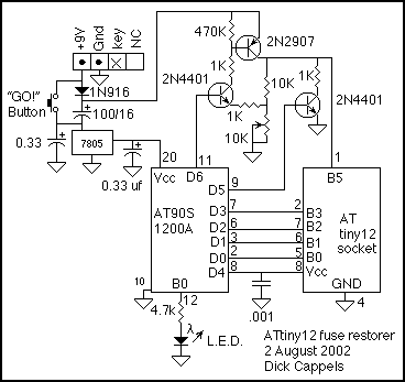
Plug an ATtiny12 into the 8 pin socket and hold down "GO!" button. The LED will come on at the end of the programming process, which only takes a couple hundred milliseconds. The fuses are now restored to their...
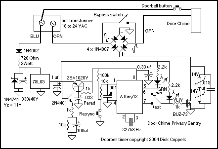
The device described here does just that. The circuit connects to the doorbell circuit, taking power from the 18 VAC from the doorbell transformer and switching power to the doorbell circuit most of the day. The user interface is...
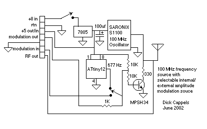
A frequency reference for tuning up the RS-232 to 100 MHz RF desktop channel adapter elsewhere on this site, when I found this Saronix crystal oscillator in my junk box. A few minutes with AVRStudio produced an ATtiny12 to...