
Common-emitter transistor amplifier quiescent bias circuit diagram
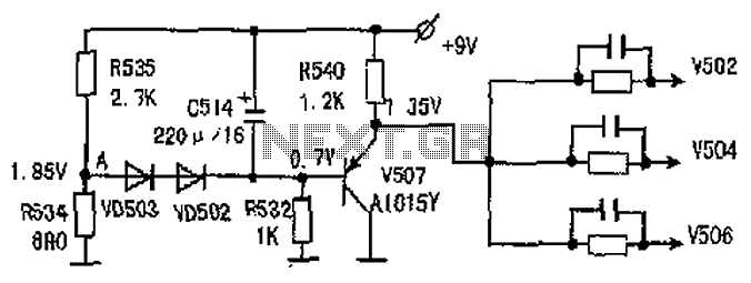
The common-emitter amplifier circuit, featuring transistors V502, V504, and V506, operates by utilizing a voltage follower configuration that stabilizes the bias voltage at the emitter. This configuration is crucial for maintaining consistent performance in video applications where brightness levels must remain stable despite variations in supply voltage. The resistors R534 and R535 are integral to creating a reliable voltage divider, allowing for precise control of the base voltage applied to the transistors V507, VD502, and VD503. The careful selection of component values ensures that the total emitter voltage remains stable, even as the input voltage fluctuates.
The role of the common base amplifier is significant in this circuit, as it directly influences the overall gain and response of the amplifier. By grounding the base through capacitor C513, the circuit allows for AC signal coupling while maintaining a stable DC operating point. This ensures that the input signals processed through V501, V503, and V505 can be amplified effectively without introducing unwanted noise or distortion.
Temperature compensation is another critical aspect of this design. The junction voltages of the diodes VD502 and VD503 are sensitive to temperature changes, and their behavior is leveraged to adjust the biasing of the video amplifier. As the temperature rises and the junction voltage decreases, the circuit compensates by allowing the emitter voltage of V507 to increase, thereby maintaining the amplifier's performance.
In summary, the circuit's design is meticulously crafted to ensure operational stability and consistency in video amplification applications. By integrating various components such as voltage followers, common-emitter amplifiers, and temperature compensation mechanisms, the circuit achieves a robust performance that meets the demands of high-quality video signal processing. Common-emitter amplifier V502, V504, V506 emitter static potential bias voltage forming circuit [ie voltage follower) shown in Figure 3. Active filter by the V507, VD502, VD503 , R534, R535, C514, R540 is composed of V502, V504, V506 emitter static bias voltage follower circuit. R535, R534 composed divider network dividing point voltage by 1.85V down to V507 VD502 VD503 string base, about 0.7V, its emitter voltage of about 1.35V or so, as the common-emitter amplifier V502, V504, V506 three only enlarge the emitter bias voltage source tube.
Common base amplifier base bias voltage directly from + 9V power supply, common base amplifier tube base by C513 AC ground, and therefore input and output signals in terms of V501, V503, V505 for the common-base circuit. Using V507 (PNP-tube) as a common-emitter amplifier video amplifier quiescent bias in the emitter voltage follower, because the video amplifier common base amplifier tubes V501, V503, V505 are connected to the base of the power supply + 9V endpoint.
A slight change in the supply voltage, will affect its quiescent operating point, the output tube collector static potential changes affecting the brightness of the screen. For this reason, the use of the circuit diagram, so that common-emitter amplifier bias voltage emitter follower + 9V power supply trace changes synchronously change, that a slight change in the + 9V power supply, V502, V504, V506 emitter voltage follower change, to ensure total emitter, common base of two transistors are not fluctuate with changes in the power trace, ie V501, V503, V505 collector static potential unchanged.
This aspect can ensure consistency of product performance in large quantities, but also to ensure that single brightness is not affected by small changes in the supply voltage. VD503, VD502 junction voltage (0.5-0.7V) decreases with increasing temperature, so that V507 emitter potential rise can be compensated video amplifier common emitter, increased two cascaded amplifiers Shenlian common base transistor with increasing temperature, causing static IMPACT operating point changes, so that the final stage amplifier video amplifier drift is reduced, job stability is greatly improved.
Since the C514 is connected between the power supply + 9V and V507 base, but also to avoid power transients caused by luminance transients.
Related Circuits
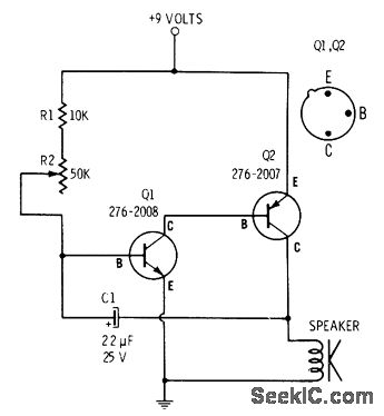
R2 controls the charging speed of capacitor C1. At a specific charge level, C1 triggers transistors Q1 and Q2, which release a 9-volt pulse. This pulse generates a clicking sound. The discharge process of the capacitor involves it charging...
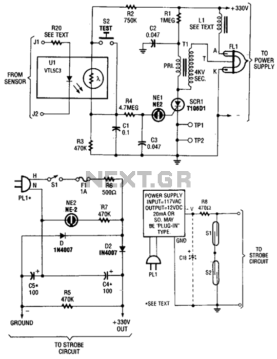
The circuit is activated by an LED/photoresistor isolator (U1), which combines a light-dependent resistor (LDR) and an LED in a single package. This device was selected for its high isolation characteristic of 2000 V, which is essential since the...
The IED functions as a hotel, restaurant, and family-oriented tool designed for the effective eradication of mosquitoes, as illustrated in Figure 16-12a. It employs a diode voltage doubler rectifier circuit to generate a high voltage. When mosquitoes are attracted...
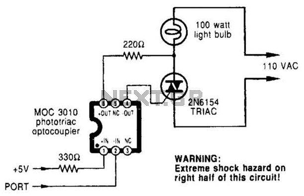
A microcomputer-to-triac interface utilizes a phototriac optoisolator to safely isolate logic signals, allowing direct control of high-power loads. This circuit can function as either an on/off switch or a proportional phase control, depending on the input waveforms and the...
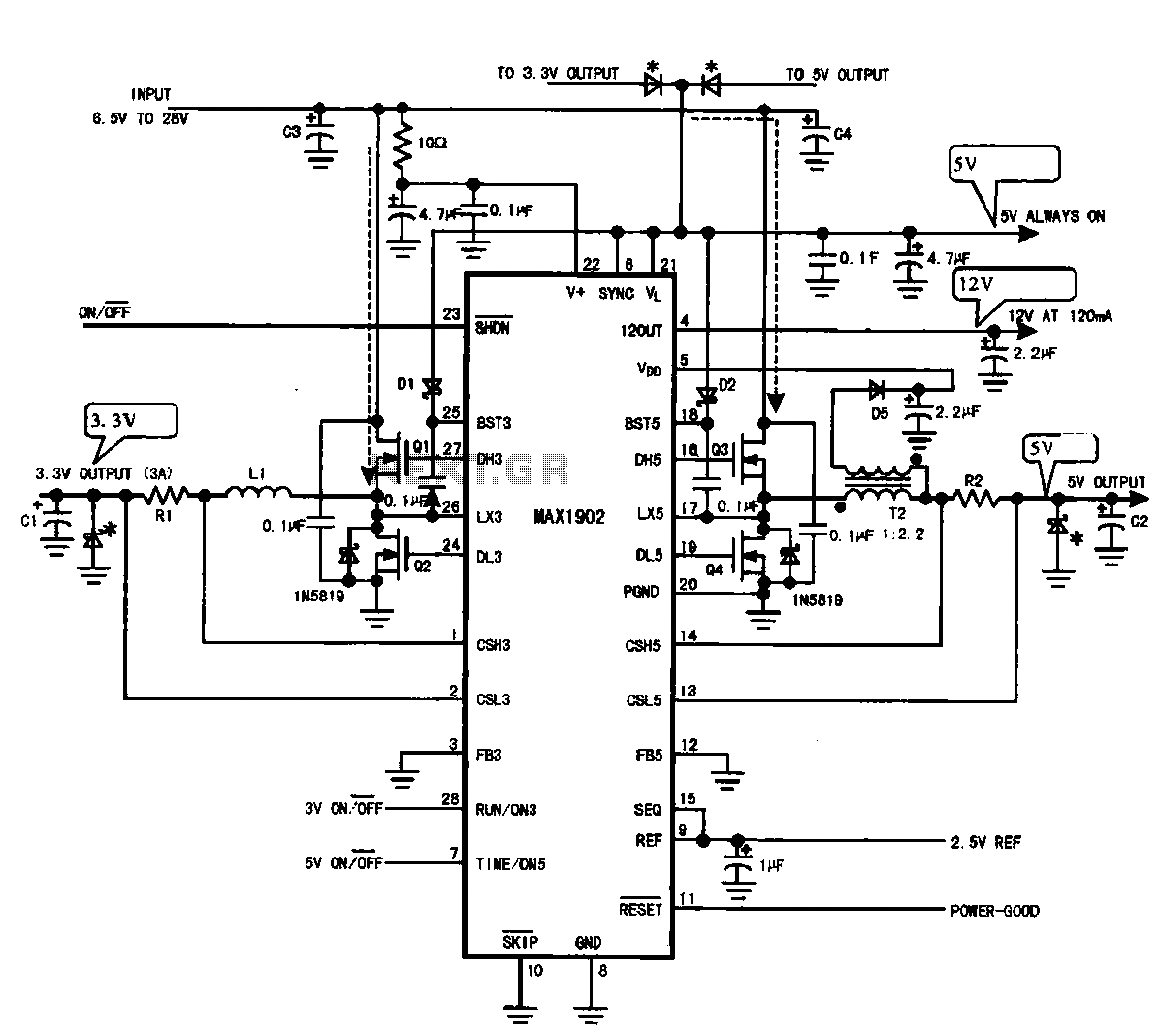
Multi-output power supply circuit (MAX1902). This circuit illustrates the power supply configuration for a notebook computer motherboard, utilizing the MAX1902 chip for power control. It is designed to convert the battery's DC voltage into multiple DC voltage outputs. The multi-output...
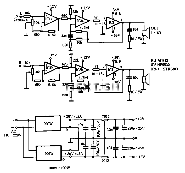
The T amplifier circuit schematic section is illustrated in Figure 3-51. It utilizes the Japan Sanyo STK6303 Pina, which is a high-power thick film integrated circuit. The maximum power supply voltage is 36V, and the output current can reach...
Warning: include(partials/cookie-banner.php): Failed to open stream: Permission denied in /var/www/html/nextgr/view-circuit.php on line 713
Warning: include(): Failed opening 'partials/cookie-banner.php' for inclusion (include_path='.:/usr/share/php') in /var/www/html/nextgr/view-circuit.php on line 713