
communication with AVR microcontroller
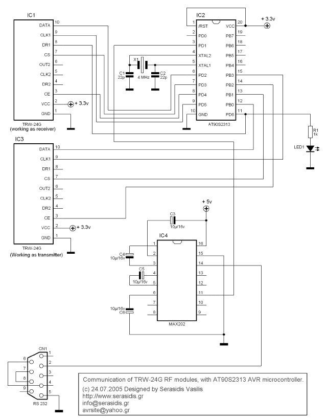
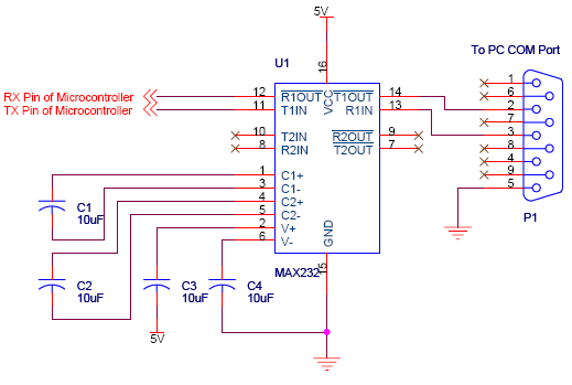
The circuit design integrates various components to facilitate the communication between the RF modules and the microcontroller. The TRW-24G modules are versatile, allowing for both transmission and reception of data, which is critical for wireless communication applications. The AT90S2313 microcontroller serves as the central processing unit, managing the data flow and configuration of the RF modules. The MAX202 level converter ensures compatibility between the microcontroller's 3.3V logic and the 5V logic of the STK500 board, enabling seamless data transmission without risk of damage to the RF modules.
The schematic should clearly depict the connections between these components, including the power supply lines, ground connections, and data lines. It is essential to ensure that the voltage levels are correctly managed, particularly for the RF modules, which require careful attention to avoid exceeding their maximum voltage specifications. The configuration process for the RF modules should also be included in the schematic, illustrating how the microcontroller sends the necessary serial bytes to set up the communication parameters.
Additionally, the timing of the data transmission and the protocols used for serial communication should be outlined in the design documentation. This includes specifying the baud rates for both the RF communication and the serial link to the PC, as well as the data format being used. Proper labeling of all pins and connections on the schematic will aid in troubleshooting and future modifications to the circuit. Overall, this design exemplifies a well-structured approach to integrating RF communication into a microcontroller-based system.The TRW-24G connector pins is too small (~1mm pin to pin). For that I order the adaptor PCB that is convert the small connector of RF module, to standard pin connector. The pin order of RF modules in schematic diagram is based on pin order of pin adaptor, andnot on pin order of the module`s connector.
My circuit is constituted by 2x TRW-24G modules, 1x AT90S2313 microcontroller and 1x MAX202 TTL to RS232 voltage level converter. The RF modules work with +3. 3V not with +5V. I connected this modules to STK500 development board and I set the VTG voltage to 3. 3V from programmer`s software in AVRstudio. For serial communication I used the internal MAX202 of STK500 board, that works at +5V power supply. There is no problem with that, but the AT90S2313 MUST work at 3. 3V or else you will burn the RF modules if you send +5V instead +3. 3V (max. 3. 6V). When you power-on this circuit, the AVRwill configure the IC1 as receiver and IC3 as transmitter. Then, the AVR will check the DR1 pin of IC1 for incomming data. If DR1 pin of IC1 is LOW (logic `0`) the AVR will send serially fromIC3the 5 byte address of the module that wants to send the data (AA, BB, CC, DD, EE hex address) and the Payload bytes which is the data thatwants to send (31, 32, 33, 34 hex, arethe same as 1, 2, 3, 4 ASCII). When AVR pushes the CE1 pin of IC3 to LOW (`0`) the IC3 transmits the data with baud rate of 250kbps (I set the communication to 250Kbps not to 1Mbps).
After some small delay, the AVR reads again the DR1 pin of IC1 for incoming data. In this step the DR1 pin of IC1 goesto logic `1` because receiver`s buffer now has the4 bytes (payload bytes) that we had transmitted before with IC3. The LED1 it will flash for a moment to show that the receiver`s buffer has incoming data. Then, the AVRwill read these 4 bytes and send them serial via PD1 and MAX202 to PC with baud rate 9600bps/8/n/1.
When AVR reads all data from IC1, the LED1 it will be turned-off. You can connect the CN1 to COM1 serial port of your PC, run the Hyperterminal (start->programs->accesories->communications->hyperterminal) and set it at COM1 with 9600bps/8/N/1. When you power-on this circuit you will see some small flash in the LED1 and after a small delay you can see the ASCII characters <1234> in Hyperterminal`s screen.
The TRW-24G modules are transmitters and receivers both. The function is dependent by the configuration of each module. When you power-on the module, you have to send 2 or 16 serial bytes to configure the modules. The method to configure this RF modules is described in this manual. 🔗 External reference
Related Circuits
Serial communication using UART or USART of a microcontroller 8051 AVR PIC, software implementation of half-duplex UART and MAX232 interfacing with microcontrollers 8051 AVR PIC. The described system focuses on implementing serial communication via UART (Universal Asynchronous Receiver-Transmitter) or USART...
For those who prefer convenience, it is possible to turn the bedroom light on or off without leaving the bed simply by clapping hands. This concept inspired the design of a clap-activated light control system. Various clap switch projects...
Rsense will cause Q2 to conduct when a threshold of approximately 0.65V is reached. Rbias will determine the extent of this limitation, although this aspect remains unclear. Particularly, if Rsense is positioned on the high side, simply activating Q2...
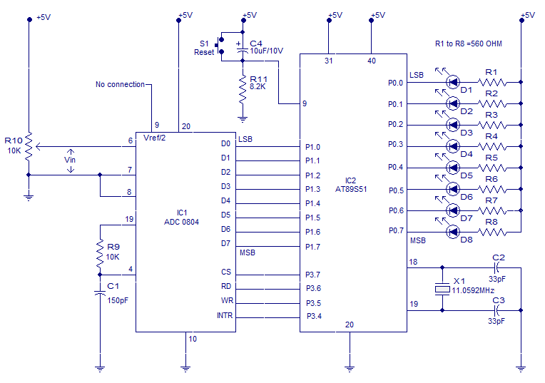
Interfacing ADC to 8051 microcontroller. ADC0804 is interfaced to microcontroller AT89S51. Complete circuit, theory and program in assembly language. The interfacing of an Analog-to-Digital Converter (ADC) with a microcontroller is a critical aspect of embedded systems design, particularly when analog...
ISP programmer with circuit diagram for AVR Atmega32 microcontroller. This ISP burner circuit is an adaptation of the Pony programmer and uses PonyProg software. The ISP (In-System Programming) programmer designed for the AVR Atmega32 microcontroller facilitates the programming of the...
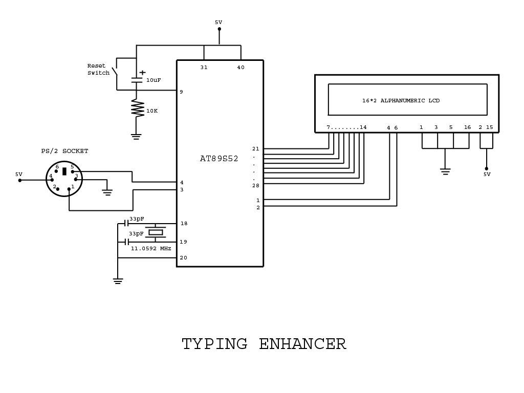
Project with Circuit and Code for a Typing Assistant using the 8051 microcontroller (AT89S52) and the PS/2 keyboard port of a computer. The project also explains the interfacing of the PS/2 port of a computer with the 8051 microcontroller. The...
Warning: include(partials/cookie-banner.php): Failed to open stream: Permission denied in /var/www/html/nextgr/view-circuit.php on line 713
Warning: include(): Failed opening 'partials/cookie-banner.php' for inclusion (include_path='.:/usr/share/php') in /var/www/html/nextgr/view-circuit.php on line 713