
Compensating the forward voltage drop of a diode signal rectifier

The circuit utilizes D1 and D2 as diodes in a biasing configuration, where D1 is responsible for establishing a stable reference voltage of 0.6V. R1 and R3 work in tandem with D1 to ensure that the bias voltage remains consistent while allowing the AC input signal to superimpose on this bias. The design ensures that D2 is on the verge of conduction, thus requiring minimal input signal variation to initiate conduction. The capacitive coupling allows the AC signal to pass while blocking any DC components, ensuring that the output reflects only the desired variations in the input signal.
The role of R2 is crucial as it helps to define the output voltage by providing a load to D2. The interaction between the input signal and the bias voltage is critical for maintaining the desired output characteristics. The choice of a larger capacitor (10µF) in the simulation allows for a better representation of low-frequency behavior, which is essential for applications requiring stable AC signals. The frequency of 1000Hz is particularly effective in this setup, as it allows for adequate coupling through the capacitor while avoiding excessive loading effects that could distort the output signal.
In summary, this circuit effectively utilizes a combination of diodes, resistors, and capacitive coupling to create a biasing mechanism that allows for efficient signal processing, ensuring that the output remains stable and responsive to the input variations while maintaining the integrity of the diode's operation.It says that D1 compensates for D2`s forward drop by providing 0. 6V of bias. Is the +5V an external 5v source How does it compensate The R1, R3 and D1 basically creates a 0. 6V bias on the other side of the capacitor, so that a positive swing in the signal does not have to overcome a0. 6V hurdle. D_1 and R_3 form a shunt voltage regulator. The 0. 6V voltage is conveyed to D2 which is on the verge of conducting, as a result. So only a small positive upswing from the input is required to bring it to conduction. Because the input is capacitively coupled, it is pure AC. Its swings are additively superimposed on top of the bias voltage that exists on the other side of the capacitor. The 5V source is just from somewhere in the rest of the circuit. There is nothing special about it. Perhaps you can get a different perspective by redrawing the circuit so that voltage falls from top to bottom.
In this view, we highlight how the input is biased to 0. 6V, but the output is 0. 6V below that, down across the voltage drop of D1. So for instance suppose that the input creates a positive swing of 0. 1V. This becomes 0. 7V at the top of D2 (the whole point of the bias). At the bottom of D2, that swing is 0. 1V again. D2 lets through enough current so that R2 has 0. 1V across it. A negative swing of 0. 1V turns to 0. 5V. But this cannot create a -0. 1V output at the bottom of D2; that is nonsense because it is outside of our supply range. 0. 5V is not enough to forward bias D2, and so the output is at 0V, pulled to ground by R2, which has almost no current flowing across it to create any voltage. The purpose of R1 is to act as a flexible linkage to separate the reference 0. 6 voltage, which is quite stiff, from the point where the signal is injected, which must on the contrary be free to swing about 0.
6V. R1 also protects the diode from the input current swings. If we replace R1 by a wire, it won`t work because the signal will try to move the voltage at the top of D1, whose cathode is pinned to ground. The input`s positive swings will dump current through D1, abusing it. That creates a poor input impedance, resulting in an inability to generate the right voltage on or under D2.
To make it nicer for simulation, let us make the capacitor way bigger: 10 uF. Then we can use a nice, low frequency like 1000 Hz, which will not pass very well through a 100 pF capacitor into a less than 1K impedance. Also, let`s hook up a signal source with a 3V amplitude. If you run the time domain simulation, you will see that the output waveform is quite precisely chopped in half.
🔗 External reference
Related Circuits
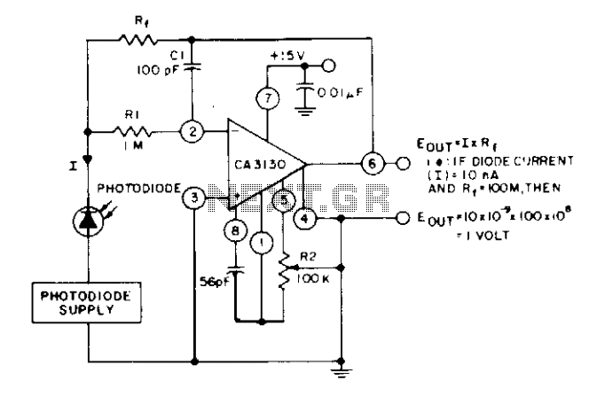
The circuit utilizes three CA3130 BiMOS operational amplifiers in an application that is sensitive to sub-picoampere input currents. It provides a ground-referenced output voltage that is proportional to the input current flowing through the photodiode. The circuit design employs three...
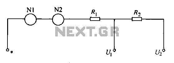
A voltmeter operates through a measuring mechanism in a specified circuit, utilizing a moving coil in series with additional resistance. The fixed coil is denoted as N1, while the moving coil is designated as N2. The additional resistances are...
The TL494 serves as the core component for a PWM driver and protection circuit operating at a frequency of 50 kHz. The output voltage of 115V is stepped down and isolated before being sent to the TL494 error amplifier...
The circuit is a MOSFET based linear voltage regulator with a voltage drop of as low as 60 mV at 1 ampere. Drop of a fewer millivolts is possible with better MOSFETs having lower RDS(on) resistance. The circuit uses...
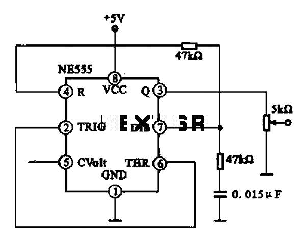
A 1 kHz square wave signal generator is created using a time base circuit with an NE555 timer, combined with a time constant circuit consisting of a 47 kΩ resistor and a 0.15 µF capacitor. The circuit utilizes the...
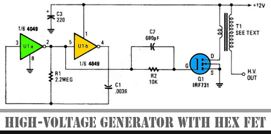
The schematic diagram below illustrates a high voltage generator circuit. This circuit employs a 4049 hex inverter configured as an oscillator, and it can utilize an ignition transformer from an automotive engine. A fly-back transformer may also be suitable....