
Complementary AC power switching
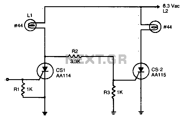
The circuit operates by utilizing two controlled switches (CS1 and CS2) to manage the energization of two loads, L1 and L2, based on an input signal. CS1 is activated by a low-level input signal of less than 1 mA and 1V, which allows it to conduct during the positive half-cycles of the anode voltage. This conduction provides half-wave rectified DC to load L1, ensuring that it receives the necessary power for operation.
The voltage divider formed by resistors R2 and R3 plays a crucial role in determining the activation of CS2. Since the maximum voltage at the anode of CS1 does not exceed 1 volt, the voltage divider does not generate sufficient voltage to trigger CS2, thus keeping L2 de-energized while CS1 is active. Upon the removal of the input signal, CS1 ceases to conduct, resulting in L1 being de-energized, although a minor amount of AC current may still flow through R2 and R3.
CS2 is designed to activate at the onset of each positive half-cycle once the anode voltage of CS1 rises to between 2 to 3 volts. When this occurs, CS2 conducts for the majority of the positive half-cycle, which allows L2 to be energized. The design of the circuit ensures that the 6-volt lamps used in this application will achieve their rated brightness due to the half-wave rectification provided by the controlled switches, significantly enhancing their operational lifespan. For applications requiring full brightness, it is recommended to increase the anode supply voltage to 9 volts AC, which will provide sufficient energy for optimal lamp performance. This circuit exemplifies an efficient method of controlling load energization through precise voltage management and switch control.An input signal of less than 1 mA and 1V is required to switch on CS1. As long as this input -signal is maintained, CS1 will conduct during each positive half cycle of anode voltage, thereby energizing load LI with half-wave rectified dc. L2 remains de-energized, since the anode of CS1 will not go more positive than 1 volts, and voltage divider R2 - R3 cannot provide enough voltage to trigger CS2.
Upon removal of the input signal, CS1 will drop out. Ll will be de-energized, except for a small amount of ac current through R2 and R3 CS2 will be triggered on at the beginning of each positive half-cycle, when CSl anode voltage reaches 2 to 3 volts. CS2 will conduct for nearly the entire positive half-cycle energizing L2. It should be noted that the 6 volt lamps used will operate at Wthe rated brilliance because of the controlled switch half-wave rectifying action and will extend the operating lamp life by several orders of magnitude.
Should full brilliance be desired, the anode supply voltage level should be raised to 9 volts ac. 🔗 External reference
Related Circuits
The LV2282VA is an FM Transmitter integrated circuit (IC). The multiplex (MPX) block generates a stereo modulated composite signal from left (L) and right (R) audio inputs. The radio frequency voltage-controlled oscillator (RF VCO) incorporates an FM modulation function....
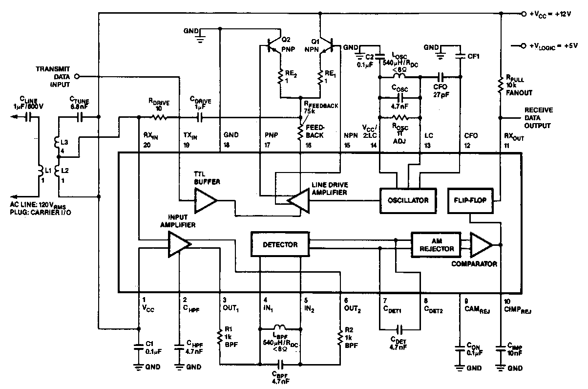
In the 100 kHz application, the coupling network connects to the receiver section located at the bottom of the chip. The external components will be summarized later. The receive data output is pulled up through a resistor (RPuLL) valued...
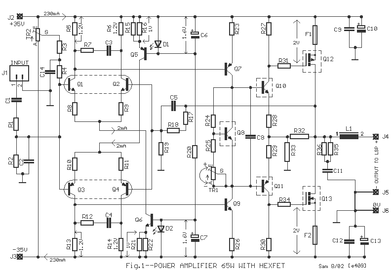
A medium power amplifier that is characterized by a lot of good sound quality, but simultaneously is very simple in the construction. It uses, enough time in active loudspeakers. In its output stage exist the very good FET transistors,...
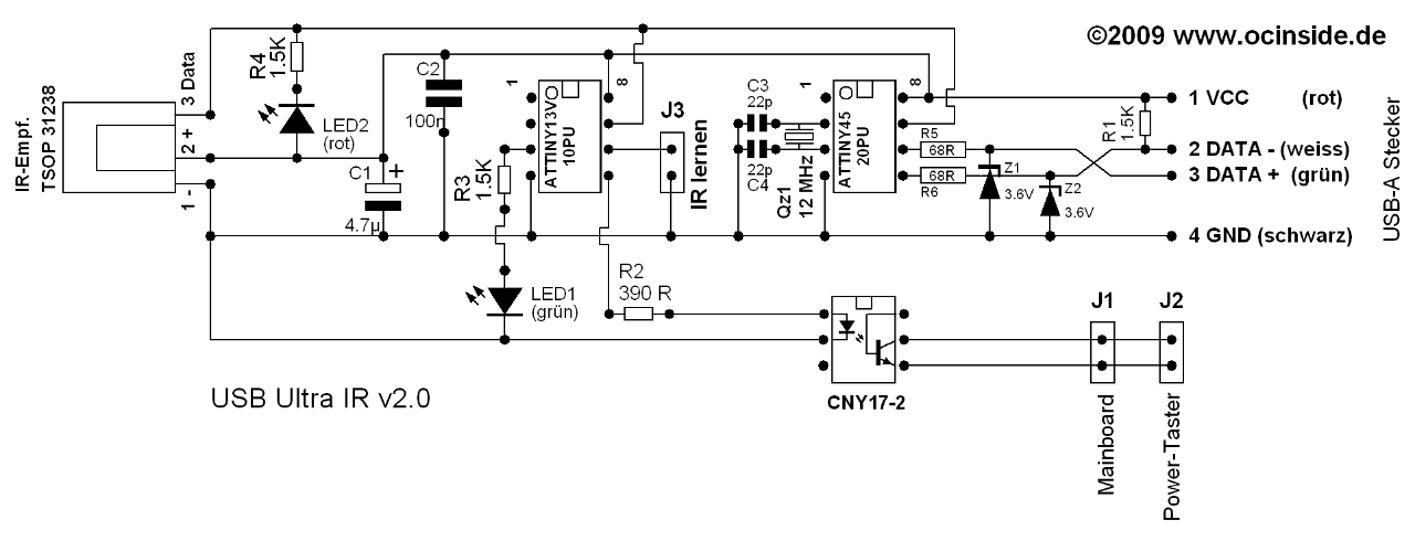
This Atmel integrated circuit operates at a clock frequency of 12 MHz, facilitating communication between an infrared receiver and a personal computer. This setup enables the processing of signals by infrared receiver software, such as Girder. When a valid...
The goals were achieved by utilizing a discrete-components operational amplifier (op-amp) driving a complementary common-emitter output stage configured for Class B operation. In this configuration, for small output currents, the output transistors remain off, allowing the op-amp to supply...
Readers who do not wish to modify the power supply of an old PC into a suitable halogen power source may find the current design a welcome alternative. The circuit does not require any alterations to the power supply....
Warning: include(partials/cookie-banner.php): Failed to open stream: Permission denied in /var/www/html/nextgr/view-circuit.php on line 713
Warning: include(): Failed opening 'partials/cookie-banner.php' for inclusion (include_path='.:/usr/share/php') in /var/www/html/nextgr/view-circuit.php on line 713