
Complementary symmetry push-pull circuit

The Class B power amplifier circuit is characterized by its push-pull configuration, which effectively reduces distortion by ensuring that each transistor only amplifies one half of the input signal cycle. This method not only enhances the overall efficiency of the amplifier but also increases the output power compared to Class A amplifiers. The operation of the transistors is controlled by the input signal, with biasing techniques employed to ensure that each transistor remains in the cutoff region when not conducting.
In practical implementations, the circuit typically includes biasing resistors, coupling capacitors, and feedback mechanisms to stabilize the gain and improve linearity. The output stage may also incorporate additional components such as output transformers or filters to match the load impedance and remove unwanted high-frequency noise. The careful selection and arrangement of these components are crucial for optimizing performance, minimizing crossover distortion, and achieving a smooth transition between the conduction of the two transistors.
Overall, the complementary symmetry push-pull amplifier offers a robust solution for applications requiring efficient amplification with manageable distortion levels, making it a popular choice in audio amplification and various electronic devices. Class A power amplifier distortion, although low, but its low efficiency and output power is small, so people designed B power amplifier circuit. B amplifier circuit is to work from the middle point Q moves down to the position Q2, that is static -free base of the transistor bias, b 00 only when the input signal is the role of the transistor is turned on before work. It works when the maximum collector current of the magnitude of the current class Bijia much larger output.
But it is only in the positive half cycle of the signal t is not a negative half-cycle work. This causes serious distortion of the output signal o this end, the B push-pull amplifier circuit uses the output of work, consisting of two alternating work tube output, l-140 one of the circuit shown by the NPN transistor VTz and a PNP tube VT3 composition. In the positive half cycle signal VT. 3 work, negative half cycle of the signal VT2 tube in two output tubes, respectively, the output signal of the positive and negative half-cycle, the last in a complete synthesis of the total output of the output signal of the circuit o taken with two different polarities its lack of complementary transistors, so this circuit is called complementary symmetry push-pull output path.
Related Circuits
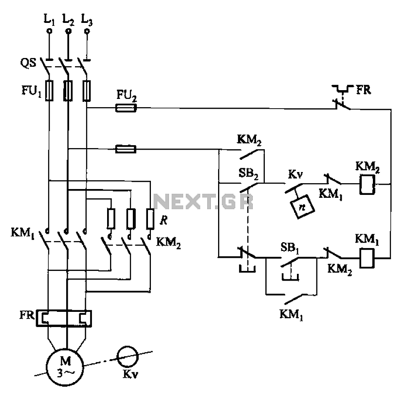
The circuit depicted in Figure 3-124 operates without an intermediate relay. Kv serves as the speed relay, activating when the electric motor speed exceeds 120 r/min while the contact is closed. If the speed drops below 100 r/min, the...
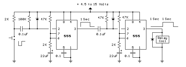
The circuit below illustrates generating a single positive pulse which is delayed relative to the trigger input time. The circuit is similar to the one above but employs two stages so that both the pulse width and delay can...
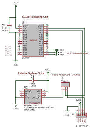
The SX 28 internal oscillator is not that fast, so an external oscillator can be hooked up to the processor as shown in the diagram to increase the operation cycles per second. The SX 28 microcontroller is designed with an...
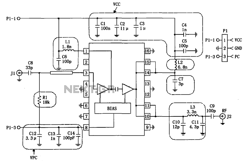
The RF2132 linear power amplifier circuit is depicted in the provided figure. A radio frequency (RF) signal enters through input pin 3 and is processed via a preamplifier. The final stage of the amplifier outputs a gain of 10....
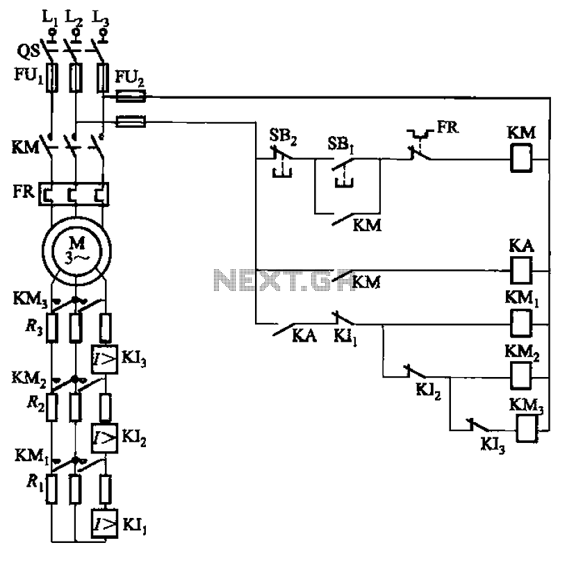
The circuit illustrated in Figure 3-161 features a first stage current detection mechanism utilizing a current relay (KI1) in series with a resistor (R1). The second stage employs another current relay (KI2) in series with a resistor (R2) for...
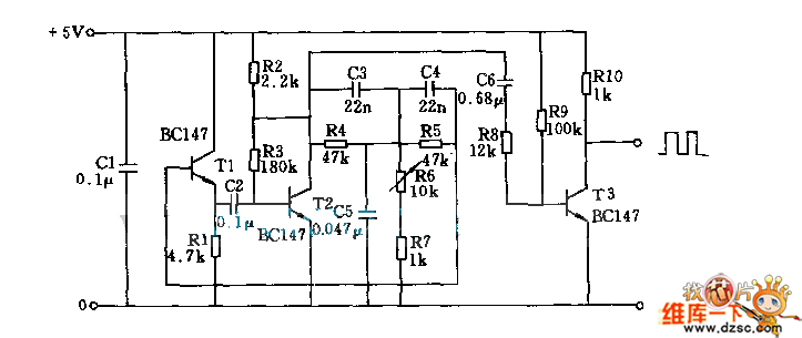
T1 and T2 in the circuit form the inherent oscillator, while T3 serves as the output stage. The network consists of a high-pass filter (C3, C4, R6, and R7) and a low-pass filter. The output from this network is...