
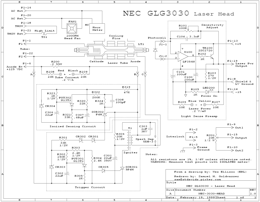
Complete Ar/Kr Ion Laser Power Supply Schematics
The circuit operates in a highly integrated manner, ensuring efficient control of the laser tube current through a feedback mechanism. The use of opto-couplers for isolation between the outer and inner loops enhances safety and stability, particularly in high-voltage applications. The feedback amplifier's design allows for precise regulation of the tube current, with the frequency response tailored to effectively manage transient conditions and noise. The incorporation of a clipping diode serves as a protective measure, preventing instability during high current conditions. The unique operational characteristics of the TL494 controller, functioning in an inverted mode, facilitate effective power management while maintaining high efficiency. Overall, this design exemplifies a robust approach to managing laser tube currents in power supply applications, ensuring reliable performance across varying operational states.The circuit is split into two sections: the isolated external loop which is connected to the remote interface connector on the front of the PSU and the non-isolated inner loop which is connected to the HT (AC line) supply. The two loops are linked by opto-couplers OK1 and OK2. Initially the outer loop is inactive and all regulation takes place wit hin the inner loop, this is also the case when the power supply is set to standby mode via the remote connector. R47 is in series with the anode of the laser tube, when current flows, the current mirror consisting of Q1 to Q5 produces a voltage across 100 ohm resistor R51, this is approximately 130 mV/A of tube current.
This monitor signal is fed into IC3d which then drives opto-coupler OK2 which feeds the current signal into the isolated outer loop. The current signal is also fed into the feedback amplifier consisting of IC3c, IC3a and associated components.
This amplifier has a flat frequency response between 0 and 1 Hz, and then rolls off by 3dB to 10 Hz and is flat again to 10 kHz where it then rolls off at 3dB/octave. Diode D8 appears to be present to clip the signal should fast transients appear in the current signal.
Without the diode installed, the tube and power supply become unstable above 8 A (more on this later). IC3a is AC coupled and feeds the noise component of the tube current back to the first amplifying stage via R28, the noise control adjustment.
R27 sets the standby current to, nominally, 4 A. R26 controls the gain of the circuit when regulating on the outer loop. OK1 is initially switched off so the top of R26 is nominally 0V therefore the feedback amplifier output depends only on the setting of R27 and the tube current signal. The feedback signal output from IC3c feeds into one of the error amps in IC4, a TL494 SMPS controller; IC4`s outputs are in parallel and drive IC5, a DS0026 MOS inverter/driver which, in turn, drives the MOSFETs Q6 to Q8.
As a result, IC4 is operated in an unusual inverted mode whereby the switching FETs are conducting when the output of IC4 is off, so the feedback signal goes into the non-inverting input of the error amp. The internal oscillator of IC4 runs at 100 kHz, determined by R54 and C18. And because the output control pin is grounded, the PWM output from the device is also at 100 kHz. Note that the ground of IC4 is connected to the -15 VDC power rail not 0 V. This means that the operating region for regulation is when pin 16 is between -11. 5 V and -14. 5 V. When the voltage here is more negative than -11. 5 V, the outputs of IC4 switch off causing the FETs to switch on and thus send maximum current through the tube; this current is limited only by the internal resistance of the HT supply circuit, the Rds of the FETs, the 2 current sense resistors (1 in the laser head) and the cabling resistance.
Prior to tube ignition, IC3c`s inverting input is negative with respect to the non-inverting input. The actual voltage depending on the setting of R27. IC3c runs open loop at DC so the output swings to the +15 VDC rail therefore causing the switching FETs to be turned on. This protects the FETs from any stray transients from the igniter circuit and the high di/dt waveform through the inductors.
When the tube strikes, the current very rapidly rises to around 25 A, then falls slightly to about 18 A. As a result, the current monitor signal is at around +2. 3 V and IC3c`s inverting input now becomes positive with respect to the non-inverting input, therefore the output of IC3c starts to fall to the -15 VDC rail at a rate largely determined by C8 as D8 is now conducting and damping the response of IC3c (see starting problem below); when the voltage reaches -11.
5 V the SMPS starts to regulate and the tube current reduces until the inverting input of IC3c reaches 0 V, the PSU is now in closed loop control at the standby current. The current monitor signal, isolated by OK2, feeds 🔗 External reference
Related Circuits
A simple tool to check the degree of radiation from an electric or electronic instrument. The LEDs in the circuit will provide a running light pattern when the circuit detects electromagnetic radiation from the device. It can identify radiation...
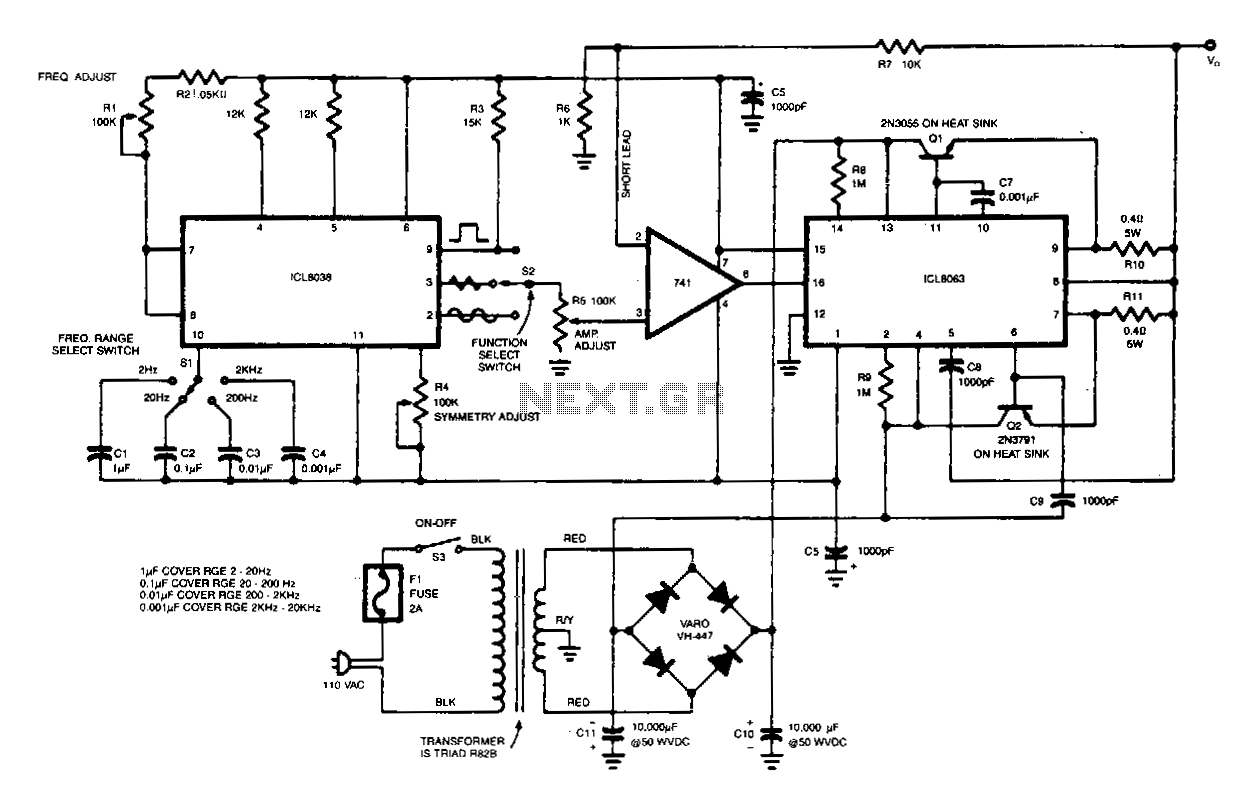
This generator is designed to produce sine, triangular, and square waves within a frequency range of 2 Hz to 20 kHz. It operates as a complete test instrument that can be connected to a standard 110 Vac power supply....
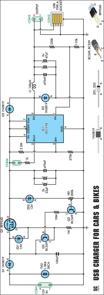
An efficient USB charger designed to operate from a 12V car battery, achieving up to 89% efficiency and capable of charging USB devices at currents up to 525mA. It does not drain the battery if left permanently connected, provided...
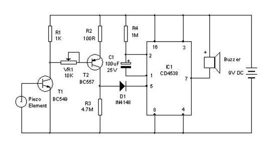
A vibration sensor or piezoelectric vibration sensor circuit diagram. It emits a loud beep when an attempt is made to break a door or window. The alarm automatically ceases after three minutes. The circuit utilizes a piezo element as...
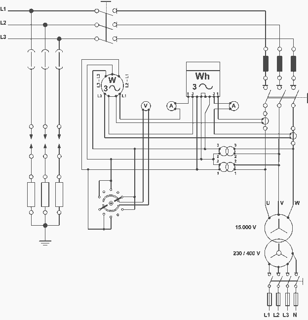
A distribution substation is defined by the apparent power of the transformer and its configuration, which can be aerial, terrestrial, or underground. A distribution substation plays a critical role in the electrical power distribution network. It serves as a point where...
This article is intended for individuals interested in constructing their own car amplifier. The fundamental calculations will be discussed below. Understanding these concepts will enable the construction of a car amplifier independently. The challenge in designing a car power...