
The Design of Car Audio Power Amplifier
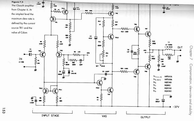
The first stage of the amplifier receives the input audio signal along with a Negative Feedback (NFB) signal from the amplifier's output. Feedback is utilized to stabilize the audio amplifier, akin to the gain factor. In a design with discrete transistors, both signals are fed to the bases of the transistors, similar to the configuration in operational amplifiers. The input signal, originating from a car radio or CD player, typically has a low voltage of approximately 1Vpp with a few milliamperes of current. To generate 170 Watts at a 4 Ohm speaker load, the signal must possess a magnitude of 28Vpp and a current of 6.5A (calculated using P=I²*R = V²/R). The first stage processes this signal at the non-inverting input, while the inverting input receives the NFB signal to ensure that the voltage gain of the amplifier remains constant, for instance, at 28 times. The output signal from the first stage does not reach 28Vpp; instead, it closely resembles the input voltage.
The second stage amplifies the voltage produced by the first stage. It is designed to amplify the voltage to yield a signal enlarged by 28 times, resulting in a 28Vpp signal from the initial 1Vpp signal. However, this 28Vpp signal still carries a small current, only a few milliamperes, insufficient to drive the speaker load. The third stage amplifies the current from a few milliamperes to 6.5A. The explanations provided for the three stages are simplified, as real amplifiers must adhere to the principles governing transistor gain, defined as G=RC/RE. This principle must be applied to each transistor within the three amplifier stages.
The first stage design incorporates a Constant Current Source (CCS), which is essential for maintaining stable operation. According to basic electronic laws, the voltage drop across the base and emitter (Vbe) equals the voltage drop across a diode, approximately 0.67V. In the CCS, the voltage drop across two IN4148 diodes equals 1.34V. The current through the CCS varies between 1-4mA. Before discussing the second and third stages, it is important to understand the amplifying effect of a transistor. The Common Emitter Mode (CEM) circuit amplifies voltage, while the Common Collector Mode (CCM) circuit serves as a current amplifier without voltage amplification.
The second stage is responsible for the maximum voltage swing in an audio power amplifier, often referred to as the Voltage Amplifier Stage (VAS). This stage consists of a voltage amplifier (CEM transistor) at the bottom, a CCS at the top, and a bias control circuit in the middle. The CCS in the second stage typically operates with a current magnitude between 4-8mA. An important component in this stage is the Miller Capacitor (CC), which defines the frequency response pole of the audio amplifier. The bias control circuit consists of a transistor, resistor, and variable resistor, typically placed on a heatsink for effective thermal management.
The third stage, or output stage, acts as the current amplifier. It, along with the bias circuit, determines whether the amplifier operates in Class A, Class AB, or Class B mode. Most car audio power amplifiers operate in Class B due to its efficiency and lower heat generation, which is critical to prevent amplifier failure. Various configurations for the output stage exist, each with a different optimum bias voltage depending on the number of Vbe drops encountered.
When connecting the three stages, the resulting circuit can be analyzed. The value of the Negative Feedback (NFB) resistor is determined by calculating the gain factor using the equation Gain = 1+(R10/R8). The output of the differential pair is tapped from the collector and sent to the VAS, which is configured as a Darlington pair. The output power stabilizer components are crucial for maintaining amplifier stability. Car power amplifiers are typically loaded with low impedance speakers, often 4 ohms, which can drop to ½ ohm in bridge mode, leading to the term "High Current Amplifier."
For building a car power amplifier, a symmetrical power supply (+, 0, -) is necessary, achieved through a DC-DC converter. The discussed converter will be of the SMPS (Switch Mode Power Supply) type using PWM (Pulse Width Modulation). This system maintains a stable output voltage, regardless of input voltage fluctuations (typically ranging from 9-15V DC).
The SMPS operates by generating voltage pulses that, when filtered through appropriate inductors and capacitors, produce a steady voltage output. The PWM technique allows for varying pulse widths to control the output voltage effectively. The design utilizes regulating PWM ICs such as TL494, TL594, SG3524, or SG3525, which compare the output voltage with a reference voltage and adjust the pulse width accordingly.
In summary, the construction of a car amplifier involves a detailed understanding of the amplifier stages, feedback mechanisms, and power supply requirements. Proper design and component selection are essential for achieving desired performance and reliability in automotive audio applications.This article is for those who wants to make their own car amplifier. The basics of calculation will be discussed below. If you have understand it you will be able to make car amplifier yourself. Actually the difficulty of designing the car power amplifier does not lies with the audio power amplifier, but it is more to providing the switching power supply. where Vpp= peak to peak supply voltage, Rl is the speaker impedance load. For car voltage of 12Vdc, if we connect it to 4 Ohm speakers we will only have power of 144/32 = 4, 5 Watt. Bridging the amplifier will double the power, but will never be more than 40 W. If we want to make more powerful amplifier, lets say 170 watt at 4 ohm speaker load, we will need supply voltage of 74Vpp, or +/- 37 Vdc.
The way to have this voltage from car supply of 12VDC is to make DC-DC converter. First stage is the stage that receives the input audio signal and Negative Feedback (NFB) signal from the output of the amp. Feedback is the back signal used to stabilized the audio amplifier, like the gain factor. For first stage built by discrete transistors, both signals is fed to basis of the transistor, like in fig1.
Both basis of the transistors is the Non- Inverting input and Inverting Input, like those in the op-amp. We can explain those stages in a simple way like this : Input signal, like from car radio or CD player have low voltage, about 1Vpp with few milliampere current.
To produce power of 170 Watt at 4 ohm speaker load, than the signal has to have maginitude of 28Vpp and current of 6. 5A (from the equation of P=I2*R = V2/R) The first stage receives this signal in the non-inverting input and the inverting input receives NFB signal to make sure the voltage gain that the amplifier produces has a constant number, lets say 28 x.
The output signal from the first stage has not reach 28Vpp, it tends to have the magnitude similiar to the input voltage. Second stage amplifies the voltage that the first stage generates. Second stage will amplifies the voltage to produce a signal that is enlarge 28x for the amplifier to have a 28Vpp signal from 1Vpp signal, but this 28Vpp signal still have small current, only a few mA and cannot drive the speaker load.
The third stage amplifies the current from few mA to 6. 5 A. Offcourse the explenation for three stages above is not that simple in the real amplifier. We should take the nature`s law for a transistor gain, that is G=RC/RE. This principles must be applied in each transistor in those 3 amplifier stages. First stage designs have main component, that is Constant Current Source (CCS) which can be seen in fig2. One of the basic of electronic law that works on every circuit is that the voltage drop of Basis and Emitor (Vbe) equals the drop voltage of one dioda = 0.
67V. It can be seen in fig2 that the voltage drop of 2 dioda IN4148 = 2 x 0. 67V = 1, 34V. We can see in RE and Q1, then V=0, 67 is substracted by Vbe of Q1 and the other 0, 67V will be the drop of RE. So we will have a Constant Current Source of 0, 67/RE. In fig2 the Ic is = 4, 4mA. CCS first stage varies between 1-4mA. Before we discuss Second Stage and Third stage, first we will discuss the amplifying effect of a transistor.
In fig3a we will see a circuit of Common Emitor Mode (CEM). This circuit will amplifies the voltage. In fig3b we see a Common Colector Mode (CCM). This circuit is the current amplifier without voltage amplifier. So if we want to amplifies voltage we use CEM circuit and to amplifies current we use CCM circuit. The Second stage responsibles for all voltage gain (Maximum Voltage Swing) in an audio power amplifier. This is why the Second stage is generally known as VAS or Voltage Amplifier Stage. This stage consist of a voltage amplifier/CEM transistor(Q5 in fig1 ) in the bottom, Constant Current Source in the top, and a bias control circuit in the middle.
Second stage CCS has current magnitude between 4-8mA In the second stage there is an important capacitor for an audio power amplifier, that is Miller Capacitor (CC in fig1 ). CC defines the pole of the frequency response for an audio amplifier and the magnitude usually in small order (severalpF).
Bias control circuit consist of a transistor, resistor and a VR like in fig5. This circuit uses a transistor that is placed in the heatsink, because the transistor have good heat compensation factor (for bipolar transistors). For the amplifier that uses mosfet transistor for the final device, the bias circuit only needs potentio or dioda only because mosfets have different heat characteristic than bipolar transistors.
The bias voltage magnitude depends on the type of the third stage used, which will be discussed later. Third stage / Output Stage is the current amplifier. Third stage and the bias circuit will defines whether an amplifier works in class A, class AB or class B.
It can be said that almost 90 % of car audio power amplifier works in class B. Operation in class B does not mean that the sound produced is not good or corrupted. With good design, we will have good audio results, both from class A or class B. The choice of class B in car audio power amplifier is conected to efficiency and the heat generated. Heat generated is a very important factor, because if not considered carefully, it will lead to amplifier breakdown. Many configurations of the output stage can be seen in fig4. Each configuration has different optimum bias voltage. It depends on how many Vbe`s that have to be passed. Example : In fig4(a) the signal has to pass 4 Vbe`s, which is Vbe Q1, Q3, Q4 and Q2. So the optimum bias = 4 x 0. 67V = 2. 8V. Both 3 stages that we have discussed above, if we connect the together will be a circuit that can be seen in fig5.
Parts of this circuit can be explained like this: - The value of Negative Feedback (NFB) resistor is determined by determining the gain factor with the equation : Gain = 1+(R10/R8) = 1+10k/500 = 21 x. The value of R10 = value of R1 to balance input. R20 and C7 are the pole and slope compensator. - The output of differential pair tapped from collector of T10 and send to VAS which is built by T12 and T4.
This configuration is called Darlington VAS and the value of R8 is standard. - R18, C6, L1 and R19 are output power stabilisator. If there is any oscilation occur in the audio power amplifier, the first tobe effected is R18 besides the final transistors. Car Power amplifier usually loaded by low impedance speakers, usually 4 ohms and can reach ½ ohm on bridge mode.
Here we know the term High Current Amplifier . The difference is the number of final transistors, or in fig5 it is the number of pairs of T7 and T8. As a rule of thumb, the number of transistor needed first has tobe calculated by equations above, and then we determine the number of final transistor needed with assumption that 1 transistor can handle 50 Watt output.
A pair of bipolar transistor can handle 100 Watt. The power is raised by parrarelling several output transistors, so the currrent flowing will be larger. For large number of final transistors, we change the predriver stage with darlington configuration. Several designs uses symetrical design, like those used in AXL and Crescendo schematic. this design is developed from the basic principal above, but the signal handling for + and - part is handled by complementary circuits.
I have an example about another kind of power amplifier, that is a non-feedback amplifier. You can view the principles of the "millenium power amplifier" in the. This amplifier has a certain gain factor in first and second stage, while the third stage is only current amplifier. For building car power amplifier, we need symmetrical power supply (+, 0, -) by building DC-DC converter.
The converter system discussed below will be the SMPS(Switch Mode Power Supply) type PWM (Pulse Width Modulation). This system will deliver stable output voltage, regardless of the input voltage (usually the car electrical system will range in 9-15Vdc).
To explain the SMPS type PWM, it can be analogued by the next example. Look at fig6. There is a voltage pulse V1 on-off with 50% wide. These pulses if passed through suitable L and C filter will be transformated into straight voltage of V2 which is V2 = ½ V1. (noticed the marked area below pulsed V1 is the same total area of the marked straight V2 ). With the same logic, if the pulse width of V1 is narrowed, we will have a lower V2 and if we enlarge the width of V1 pulse, we will have higher V2.
Some may ask, how can we get 30VDC from the car`s 12VDC The answer is simple. If we get the V1 voltage to 60VDC, then in the 50% duty cycle, we will get 30VDC straight. This is the part where the power switching transformer takes control, to make the 60VDC from 12VDC, and then chopped by the PWM. This is the princip of PWM. (Like the principal of class D digital power amplifier). In this design, we use regulating PWM IC`s, like TL494, TL594, SG3524, SG3525. These IC`s will compare the output of DC-DC converter with a reference voltage. If the output of DC-DC converter is smaller than reference voltage, then the IC will enlarge the pulse width so the voltage will raise equally to to reach determined voltage.
So as if the output of DC-DC converter is higher than the reference voltage, the IC will narrow the pulse width so the output voltage will be lowered to the determined voltage. Generally SMPS used in car audio amplifier is the push-pull system with switching frequency between 20-70Khz.
In push pull sytem like in fig7, Q1 and Q2 gives alternating switched current pulses so the transformator will be objected to maximum flux swing change without saturating the core. In this design we will use PWM IC with SG3524 from SGS Thompson. Specifications can be seen in SGS Thompson`s website. Fig8 shows the configuration of 16 pins on this IC. To make is simpler, lets design a SMPS by explaining the function of each pin. 1. First we make the Remote Turn On circuit, which is connected from the car radio / CD player. The circuit can be seen in fig9a. This circuit will turn on the SMPS by giving 12Vdc to pin 12, pin 13 and pin 15. 2. The SMPS switching frequency is determined 50Khz. For this, the clock inside IC SG3524 is adjusted 2 x 50 Khz = 100Khz. This clock is built up by pin 7(Ct) and pin 6(Rt). The approach can be done with equation Fclk = 1 /(Rt x Ct). Here we use Ct = 1nF and Rt = 10Kohm like in fig9b 4. Pin 1(Inv In) is the output voltage detector. Pin 1 is connected to the optoisolator type 4N35 like in fig9b. Optoisolator is an important component in making this SMPS so we can have Floating Secondary Ground which will prevent noises (especially whine/storing) if the power amplifier is placed in car.
The value of zener diode is 2 x 37V = 74V. If it is difficult to have zener voltage of 74 V, then we can series several zener values until we have total of 74 V. 9. For output filter capacitor of 2. 200uF, we will need approximately 4x 2. 200uF or 8. 800uF in the SMPS`s input 12Vdc. The larger the value of this capacitor, more energy stored for the SMPS. 10. Output filter inductor Lo is determine by : Lo = 0, 5 x Vout/ (I x F). With Vout = 2 x 37V = 74V, I = 8A dan F = 50Khz, we will have Lo = 0, 092mH or Lo = 0, 046mH on each supply rail + and 37Vdc.
11. Pin 11 and pin 14 are output pins that will drive the primary winding switching mosfets. Inside IC SG3524 both pins have already opereated in mode push-pull. The circuit for driving power mosfets can be seen in fig9b. The number of power mosfet used is 3 in each transformator primary. So total there is 6 power mosfets type BUZ11. 12. Transformator(trafo) for SMPS is selfwould from ferrite toroidal core (like donuts) like in fig10. It is very important that for SMPS frequency above 20Khz, we cannot use iron core transformator like we use in homes. The ferite core transformator will have black color like in the speaker magnets, but do not have magnetizing force.
The basic of equation for switching power supply with 12Vdc input is: (1) Np = 1, 37 x 105 / (F x Ae), where Np= primary number of turns, F = switching frequency, Ae = X x Y = window area of ferrite in cm2. not exceed 2A of 12VDC line. 🔗 External reference
Related Circuits
RF Power Amplifier 1 Watt. Jams Cellular Downlink Band: 800-950 MHz. The RF power amplifier described is designed to operate within the cellular downlink frequency range of 800 to 950 MHz, delivering an output power of 1 Watt. Such amplifiers...
Interfacing high power loads can be accomplished in various ways, including the use of voltage divider resistors, transformers, or optocouplers. The circuit illustrated below employs the optocoupler method. This optocoupler facilitates logic level translation with flexible input, accommodating a...
This is a low noise amplifier with a typical noise figure of 3 dB and approximately 10 dB of gain, operating within the frequency range of 450-470 MHz. It is designed for VHF two-way applications. The described low noise amplifier...
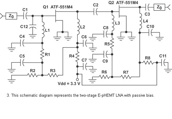
This two-stage design utilizes enhancement-mode pHEMT device technology to support IEEE 802.11a, HiperLAN2, and HiSWANa local-area network receivers. The two-stage design is characterized by its use of enhancement-mode pHEMT (pseudomorphic High Electron Mobility Transistor) technology, which is essential for achieving...
Both circuits can synchronize trapezoidal wave voltage, which is converted into intermittent small rectangular pulses. Its working principle involves periodic operation in synchronization with the grid frequency of the zero-volt switching voltage of the DC chopper. Due to the...
The signal from a synchro receiver or a variable resistive cam follower (potentiometer) is amplified by operational amplifier U1, with its output swing restricted by back-to-back zener diodes D3 and D4. This amplified signal is then fed into operational...